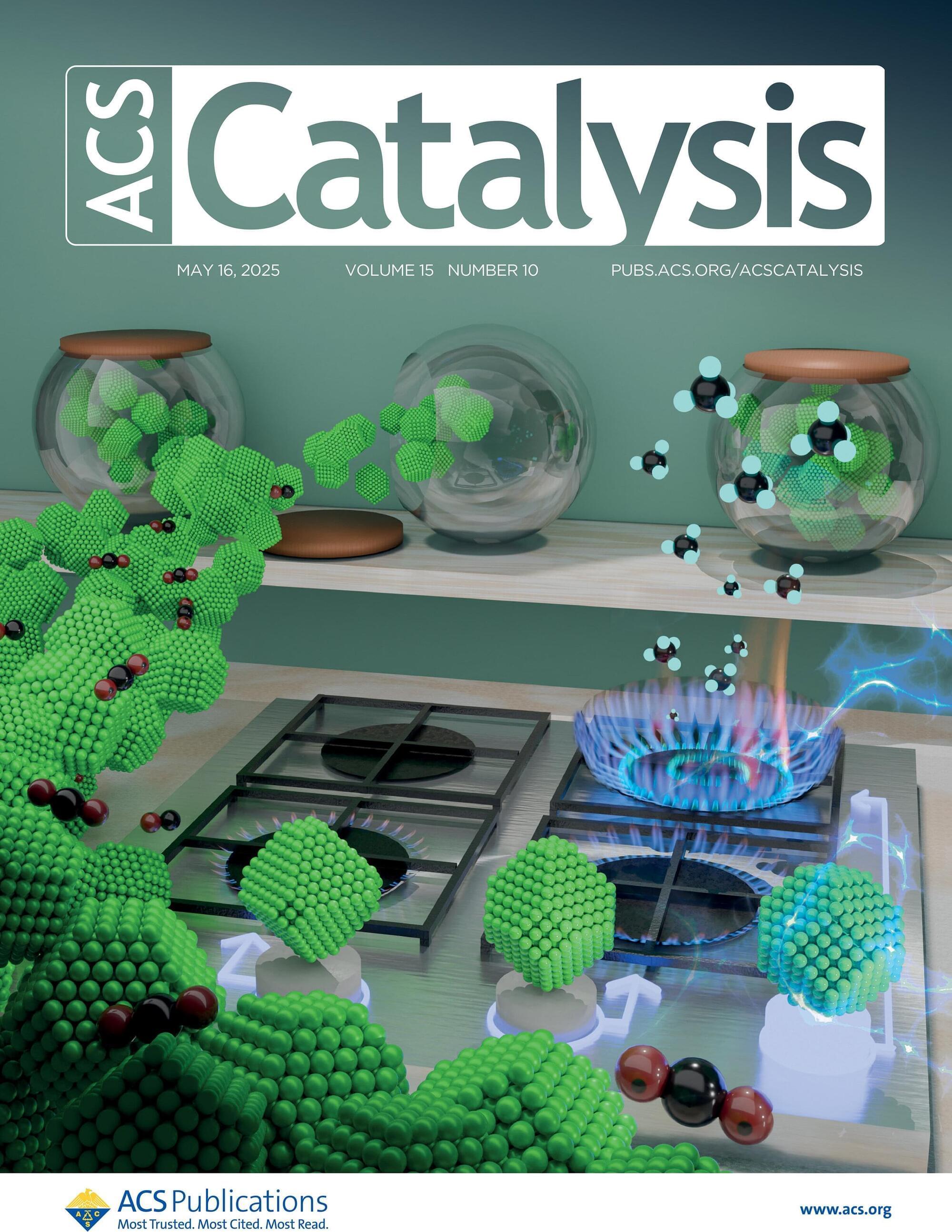
Menu

Blog

Archive for the ‘nanotechnology’ category: Page 12

Jul 2, 2024

Nanotechnology: Understanding the Tiny Science Shaping Our Future

Posted by in categories: biotech/medical, nanotechnology, science

Discover the fascinating world of nanotechnology and its impact on our lives. Learn about the science on a tiny scale and how it revolutionizes medicine, electronics, and everyday products.

Jun 29, 2024

How scientists build rotatory machines with molecules

Posted by in categories: computing, nanotechnology

Machines have evolved to meet the demands of daily life and industrial use, with molecular-scale devices often exhibiting improved functionalities and mechanical movements. However, mastering the control of mechanics within solid-state molecular structures remains a significant challenge.

Researchers at Ulsan National Institute of Science and Technology (UNIST), South Korea have made a groundbreaking discovery that could pave the way for revolutionary advancements in data storage and beyond. Led by Professor Wonyoung Choe in the Department of Chemistry at UNIST), a team of scientists has developed zeolitic imidazolate frameworks (ZIFs) that mimic intricate machines. These molecular-scale devices can exhibit precise control over nanoscale mechanical movements, opening up exciting new possibilities in nanotechnology.

The findings have been published in Angewandte Chemie International Edition (“Zeolitic Imidazolate Frameworks as Solid-State Nanomachines”).

Jun 27, 2024

Fundamental spatial limits of all-optical magnetization switching

Posted by in categories: computing, nanotechnology

Magnetization can be switched with a single laser pulse. However, it is not known whether the underlying microscopic process is scalable to the nanometer length scale, a prerequisite for making this technology competitive for future data storage applications. Researchers at the Max Born Institute in Berlin, Germany, in collaboration with colleagues at the Instituto de Ciencia de Materiales in Madrid, Spain, and the free-electron laser facility FERMI in Trieste, Italy, have determined a fundamental spatial limit for light-driven magnetization reversal.

They report their finsings in Nano Letters (“Exploring the Fundamental Spatial Limits of Magnetic All-Optical Switching”).

Modern magnetic hard drives can store more than one terabit of data per square inch, which means that the smallest unit of information can be encoded on an area smaller than 25 nanometers by 25 nanometers. In laser-based, all-optical switching (AOS), magnetically encoded bits are switched between their “0” and “1” state with a single ultrashort laser pulse. To realize the full potential of AOS, particularly in terms of faster write/erase cycles and improved power efficiency, we thus need to understand whether a magnetic bit can still be all-optically reversed if its size is on the nanoscale.

Jun 27, 2024

Advances in the study of the structure that is formed around gold nanoparticles

Posted by in categories: biotech/medical, nanotechnology

Gold nanoparticles have been the subject of intense research for several decades due to their interesting applications in fields such as catalysis and medicine. “Surface ligands” are organic molecules typically present on the surface of gold nanoparticles. During synthesis, these surface ligands play an important role in controlling the size and shape of the nanoparticles.

For several decades, the CIC biomaGUNE team led by Ikerbasque Research Professor Luis Liz-Marzán has studied in detail the growth mechanisms and properties of these nanoparticles. Despite numerous advances that have recognized the importance of surface ligands, many questions remain about their exact behavior during and after growth. Direct observation of surface ligands and their interface with gold nanoparticles has therefore been a long-standing goal for many scientists in this field.

Transmission Electron Microscopy (TEM) is the technique most widely used to investigate nanoparticles. However, the study of surface ligands by means of TEM presents significant challenges; the reason is that the ligands are sensitive to the electron beam, their contrast is limited and their structure in vacuum differs from their native state in solution.

Jun 27, 2024

Time-compression in electron microscopy: Terahertz light controls and characterizes electrons in space and time

Posted by in categories: nanotechnology, particle physics, quantum physics

Scientists at the University of Konstanz in Germany have advanced ultrafast electron microscopy to unprecedented time resolution. Reporting in Science Advances, the research team presents a method for the all-optical control, compression, and characterization of electron pulses within a transmission electron microscope using terahertz light. Additionally, the researchers have discovered substantial anti-correlations in the time domain for two-electron and three-electron states, providing deeper insight into the quantum physics of free electrons.

Ultrafast electron microscopy is a cutting-edge technique that combines the spatial resolution of traditional electron microscopy with the of ultrafast femtosecond laser pulses. This powerful combination allows researchers to observe atoms and electrons in motion, capturing dynamic processes in materials with unparalleled clarity. By visualizing these rapid events in space and time, scientists can gain deeper insights into the fundamental mechanisms that govern and transitions, helping to create advancements in research fields such as nanotechnology, optics, materials science, and .

Although ultrafast electron microscopy enables, in principle, the observation of atomic and electronic motions on fundamental spatial and temporal scales, capturing these rapid dynamics has remained challenging due to the limitations in electron pulse duration. The current standard electron pulses, lasting about 200 femtoseconds, are too long to resolve many fundamental reaction processes in materials and molecules. Pulses ten times shorter would be required to observe basic reaction paths and collective atomic motions, so-called phonon modes, in real time.

Jun 27, 2024

Quantum Leap: Ultrafast Light Unlocks New Properties in Low-Dimensional Materials

Posted by in categories: nanotechnology, particle physics

Researchers have identified new characteristics of layered low-dimensional materials that enable rapid transfers of electrons and thermal energy, pointing to potential improvements in ultrafast optical technologies and various other applications.

In a collaborative work in the Dynacom framework (French Japanese Laboratory), recent studies have highlighted that materials composed of layered tubes, which are atomically thick and classified as low-dimensional materials, exhibit new properties. Although the static properties of these structures, such as electrical conduction, are well documented, their dynamic properties, including electron transfer between layers and atomic motion triggered by light exposure, have received less attention.

In this study, scientists constructed nested cylindrical structures by wrapping carbon nanotubes (CNTs) in boron nitride nanotubes. They then examined the motion of electrons and atoms induced by ultrashort light pulses on a one-dimensional (1D) material. Electron motion was monitored using broadband ultrafast optical spectroscopy, which captures instantaneous changes in molecular and electronic structures due to light irradiation with a precision of ten trillionths of a second (10−13 s). Atomic motion was observed through ultrafast time-resolved electron diffraction, which similarly achieved monitoring of structural dynamics with ten-trillionth-of-a-second accuracy.

Jun 26, 2024

Engineers create world’s thinnest wire stable at 0 Kelvin

Posted by in categories: materials, nanotechnology

The team wondered if they could somehow leverage crystalline structures to identify a perfect candidate, sans building thousands of them in a lab.

The researchers were mostly on the lookout for 3D crystals with the right structural and electronic properties, so they could be “exfoliated.” 2D materials like graphene were extracted using this process from 3D.

Continue reading “Engineers create world’s thinnest wire stable at 0 Kelvin” »

Jun 25, 2024

Low power nanoscale S-FED based single ended sense amplifier applied in integrate and fire neuron circuit

Posted by in categories: nanotechnology, neuroscience

Motaman, S., Ghafouri, T. & Manavizadeh, N. Sci Rep 14, 10,691 (2024). https://doi.org/10.1038/s41598-024-61224-x.

Download citation.

Jun 25, 2024

New organoid culture method can verify human toxicity of nanomaterials

Posted by in categories: biotech/medical, nanotechnology

The organoids were treated with zinc oxide nanoparticles (ZnO NPs), which are a liver toxic material, and nontoxic gold nanoparticles (AuNPs). The comparison showed that the toxicity of each material could be accurately observed, in contrast to the conventional method.

Ahruem Baek, a senior researcher at KRISS, said, “Based on our results, we will establish standard nanomaterial and nanomedicine safety assessment procedures using organoids, contributing to the advancement of Korea’s nano-industry.”

The results from this study may allow for rapid and accurate safety assessment of nanomaterials and nanomedicine using organoids, contributing to the safe utilization of nanomaterials in various strategic technical fields.

Jun 25, 2024

Neuromorphic nanoelectronic materials

Posted by in categories: biological, chemistry, nanotechnology, quantum physics, robotics/AI

Memristive and nanoionic devices have recently emerged as leading candidates for neuromorphic computing architectures. While top-down fabrication based on conventional bulk materials has enabled many early neuromorphic devices and circuits, bottom-up approaches based on low-dimensional nanomaterials have shown novel device functionality that often better mimics a biological neuron. In addition, the chemical, structural and compositional tunability of low-dimensional nanomaterials coupled with the permutational flexibility enabled by van der Waals heterostructures offers significant opportunities for artificial neural networks. In this Review, we present a critical survey of emerging neuromorphic devices and architectures enabled by quantum dots, metal nanoparticles, polymers, nanotubes, nanowires, two-dimensional layered materials and van der Waals heterojunctions with a particular emphasis on bio-inspired device responses that are uniquely enabled by low-dimensional topology, quantum confinement and interfaces. We also provide a forward-looking perspective on the opportunities and challenges of neuromorphic nanoelectronic materials in comparison with more mature technologies based on traditional bulk electronic materials.

Page 12 of 300First910111213141516Last