Menu

Blog

Archive for the ‘nanotechnology’ category: Page 11

Jul 7, 2024

Research team creates process to grow sub-nanometer transistors

Posted by in categories: computing, nanotechnology, quantum physics, space

Why it matters: Moore’s Law might not be dead after all. A new technique using nanomaterials can further miniaturize transistors, allowing fab plants to pack more of them on each chip. This research opens up new possibilities for creating advanced semiconductor devices with features smaller than current lithography techniques allow.

A South Korean research team led by Director Jo Moon-Ho of the Center for Van der Waals Quantum Solids within South Korea’s Institute for Basic Science has made a significant advancement in semiconductor and nanomaterial technology that could lead to the development of much smaller, more efficient, and more powerful electronic devices. The new technique can grow “one-dimentional” metallic nanaomaterials with widths as narrow as 0.4 nanometers for use as gate electrodes on 2D substrates. The technique promises to overcome the limitations of traditional lithography.

Integrated devices based on two-dimensional semiconductors exhibit excellent electrical properties even when thinned to atomic-scale thickness, making them promising candidates for creating ultra-thin, high-performance electronic devices. A separate study indicates that these 2D logic circuits are promising candidates for the post-Moore’s Law era.

Jul 6, 2024

Sound Science: How Phononic Crystals are Shaping Quantum Computing

Posted by in categories: computing, genetics, information science, mobile phones, nanotechnology, quantum physics, science

Researchers have developed a genetic algorithm for designing phononic crystal nanostructures, significantly advancing quantum computing and communications.

The new method, validated through experiments, allows precise control of acoustic wave propagation, promising improvements in devices like smartphones and quantum computers.

Quantum Computing Revolution

Jul 6, 2024

A 2D Device May Help Quantum Computers Stay Cool

Posted by in categories: computing, nanotechnology, quantum physics

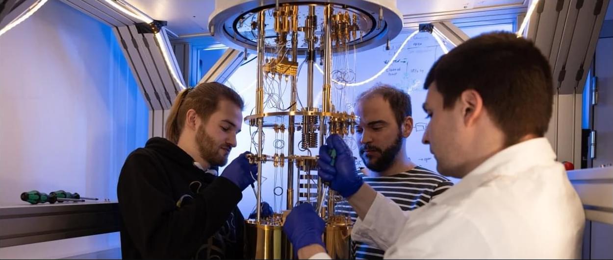
PRESS RELEASE — To perform quantum computations, quantum bits (qubits) must be cooled down to temperatures in the millikelvin range (close to-273 Celsius), to slow down atomic motion and minimize noise. However, the electronics used to manage these quantum circuits generate heat, which is difficult to remove at such low temperatures. Most current technologies must therefore separate quantum circuits from their electronic components, causing noise and inefficiencies that hinder the realization of larger quantum systems beyond the lab.

Researchers in EPFL’s Laboratory of Nanoscale Electronics and Structures (LANES), led by Andras Kis, in the School of Engineering have now fabricated a device that not only operates at extremely low temperatures, but does so with efficiency comparable to current technologies at room temperature.

Jul 5, 2024

Getting bacteria into line: Physicists use magnetic fields to manipulate bacterial behavior

Posted by in categories: nanotechnology, physics

Researchers at Finland’s Aalto University have found a way to use magnets to line up bacteria as they swim. The approach offers more than just a way to nudge bacteria into order—it also provides a useful tool for a wide range of research, such as work on complex materials, phase transitions and condensed matter physics.

The paper is published in the journal Communications Physics.

Bacterial cells generally aren’t magnetic, so the magnets don’t directly interact with the bacteria. Instead, the bacteria are mixed into a liquid with millions of . This means the rod-shaped bacteria are effectively non-magnetic voids inside the magnetic fluid.

Jul 4, 2024

Researchers Achieve High Vacuum Levitation of Silica Nanoparticle, Paving the Way for Future Levitation Technologies

Posted by in categories: computing, nanotechnology

Researchers achieved high-vacuum levitation of a silica nanoparticle on a photonic-electric chip, revolutionizing nanotechnology.

Jul 3, 2024

Scientists discover way to ‘grow’ sub-nanometer sized transistors

Posted by in categories: computing, nanotechnology, quantum physics, space

A research team led by Director Jo Moon-Ho of the Center for Van der Waals Quantum Solids within the Institute for Basic Science (IBS) has implemented a novel method to achieve epitaxial growth of 1D metallic materials with a width of less than 1 nm. The group applied this process to develop a new structure for 2D semiconductor logic circuits. Notably, they used the 1D metals as a gate electrode of the ultra-miniaturized transistor.

This research appears in Nature Nanotechnology.

Integrated devices based on two-dimensional (2D) semiconductors, which exhibit excellent properties even at the ultimate limit of material thickness down to the atomic scale, are a major focus of basic and applied research worldwide. However, realizing such ultra-miniaturized transistor devices that can control the electron movement within a few nanometers, let alone developing the manufacturing process for these integrated circuits, has been met with significant technical challenges.

Jul 3, 2024

Researchers discover way to ‘grow’ sub-nanometer sized transistors

Posted by in categories: computing, nanotechnology, quantum physics, space

A research team led by Director JO Moon-Ho of the Center for Van der Waals Quantum Solids within the Institute for Basic Science (IBS) has implemented a novel method to achieve epitaxial growth of 1D metallic materials with a width of less than 1 nanometer (nm). The group applied this process to develop a new structure for 2D semiconductor logic circuits. Notably, they used the 1D metals as a gate electrode of the ultra-miniaturized transistor.

This research was published in the journal Nature Nanotechnology (“Integrated 1D epitaxial mirror twin boundaries for ultra-scaled 2D MoS 2 field-effect transistors”).

Integrated devices based on two-dimensional (2D) semiconductors, which exhibit excellent properties even at the ultimate limit of material thickness down to the atomic scale, are a major focus of basic and applied research worldwide. However, realizing such ultra-miniaturized transistor devices that can control the electron movement within a few nanometers, let alone developing the manufacturing process for these integrated circuits, has been met with significant technical challenges.

Jul 3, 2024

Genetic algorithm enables precise design of phononic crystals

Posted by in categories: computing, genetics, information science, nanotechnology, quantum physics

The advent of quantum computers promises to revolutionize computing by solving complex problems exponentially more rapidly than classical computers. However, today’s quantum computers face challenges such as maintaining stability and transporting quantum information.

Phonons, which are quantized vibrations in periodic lattices, offer new ways to improve these systems by enhancing qubit interactions and providing more reliable information conversion. Phonons also facilitate better communication within quantum computers, allowing the interconnection of them in a network.

Nanophononic materials, which are artificial nanostructures with specific phononic properties, will be essential for next-generation quantum networking and . However, designing phononic crystals with desired characteristics at the nano-and micro-scales remains challenging.

Jul 3, 2024

Scientists develop silver nanoparticle sensor to detect genes causing hearing loss

Posted by in categories: genetics, nanotechnology

A team of scientists from the University of Sharjah say they have invented a biosensor capable of detecting the gene mutations responsible for the loss of hearing.

Jul 2, 2024

Novel method enhances size-controlled production of luminescent quantum dots

Posted by in categories: biotech/medical, nanotechnology, quantum physics, solar power

Luminescence refers to the result of a process in which an object absorbs light at one wavelength and then re-emits it at another wavelength. Through light absorption, electrons in the ground state of the material are excited to a higher energy state. After a certain amount of time characteristic of each excited state, the electrons decay to lower energy states, including the ground state, and emit light. The phenomenon is used in a wide array of technological applications involving highly efficient and reproducible emitting devices that can easily be miniaturized.

The materials with the highest luminescence efficiency include (QDs), currently used in high-resolution displays, LEDs, solar panels, and sensors of various kinds, such as those used for precision medical imaging. Functionalization of the surface of QDs with various types of molecules permits interaction with cellular structures or other molecules of interest for the purpose of investigating molecular-level biological processes.

QDs are semiconductor nanoparticles whose emissive characteristics are directly linked to dot size, owing to the phenomenon of quantum confinement. For this reason, monitoring and control of crystal growth during synthesis of QDs in solution permits intelligent planning of the desired luminescence.

Page 11 of 300First89101112131415Last