Toggle light / dark theme

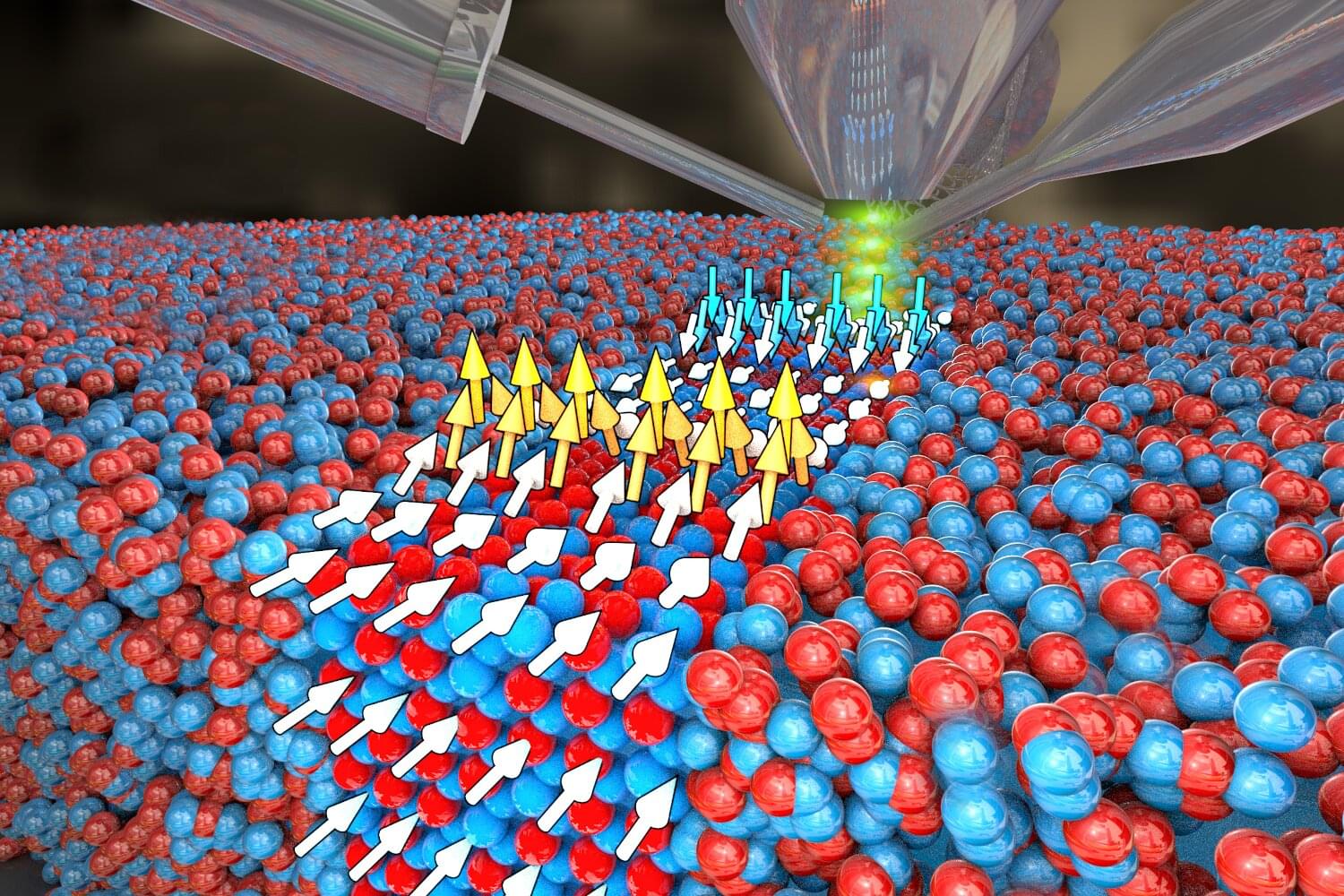
The chemical composition of a material alone sometimes reveals little about its properties. The decisive factor is often the arrangement of the molecules in the atomic lattice structure or on the surface of the material. Materials science utilizes this factor to create certain properties by applying individual atoms and molecules to surfaces with the aid of high-performance microscopes. This is still extremely time-consuming and the constructed nanostructures are comparatively simple.

Using , a research group at TU Graz now wants to take the construction of nanostructures to a new level. Their paper is published in the journal Computer Physics Communications.

“We want to develop a self-learning AI system that positions individual molecules quickly, specifically and in the right orientation, and all this completely autonomously,” says Oliver Hofmann from the Institute of Solid State Physics, who heads the research group. This should make it possible to build highly complex molecular structures, including logic circuits in the nanometer range.

Scientists have built an artificial motor capable of mimicking the natural mechanisms that power life.

The finding, from The University of Manchester and the University of Strasbourg, published in the journal Nature, provides new insights into the fundamental processes that drive life at the molecular level and could open doors for applications in medicine, energy storage, and nanotechnology.

Professor David Leigh, lead researcher from The University of Manchester, said: Biology uses chemically powered molecular machines for every biological process, such as transporting chemicals around the cell, information processing or reproduction.

Researchers leverage their understanding of molecular motors to improve nanoscale.

The term “nanoscale” refers to dimensions that are measured in nanometers (nm), with one nanometer equaling one-billionth of a meter. This scale encompasses sizes from approximately 1 to 100 nanometers, where unique physical, chemical, and biological properties emerge that are not present in bulk materials. At the nanoscale, materials exhibit phenomena such as quantum effects and increased surface area to volume ratios, which can significantly alter their optical, electrical, and magnetic behaviors. These characteristics make nanoscale materials highly valuable for a wide range of applications, including electronics, medicine, and materials science.

A research team led by scientists at Northwestern University has developed the first-ever two-dimensional mechanically interlocked material with high flexibility and strength. In the future, this could be used to develop lightweight yet high-performance body armor and other such tough materials, a press release said.

It was in the 1980s that Fraser Stoddart, then a chemist at Northwestern University, first introduced the concept of mechanical bonds. Stoddart then expanded the role of these bonds into molecular machines by enabling functions like switching, rotating, contracting, and expanding in multiple ways and using them to develop interlocked structures, which also won him the Nobel Prize in 2016.

Ferroelectrics at the nanoscale exhibit a wealth of polar and sometimes swirling (chiral) electromagnetic textures that not only represent fascinating physics, but also promise applications in future nanoelectronics. For example, ultra-high-density data storage or extremely energy-efficient field-effect transistors. However, a sticking point has been the stability of these topological textures and how they can be controlled and steered by an external electrical or optical stimulus.

A team led by Prof. Catherine Dubourdieu (HZB and FU Berlin) has now published a paper in Nature Communications that opens up new perspectives. Together with partners from the CEMES-CNRS in Toulouse, the University of Picardie in Amiens and the Jozef Stefan Institute in Ljubljana, they have thoroughly investigated a particularly interesting class of nanoislands on silicon and explored their suitability for electrical manipulation.

“We have produced BaTiO3 nanostructures that form tiny islands on a silicon substrate,” explains Dubourdieu. The nano-islands are trapezoidal in shape, with dimensions of 30–60 nm (on top), and have stable polarization domains.

University of Missouri scientists are unlocking the secrets of halide perovskites—a material that’s poised to reshape our future by bringing us closer to a new age of energy-efficient optoelectronics.

Suchi Guha and Gavin King, two physics professors in Mizzou’s College of Arts and Science, are studying the material at the nanoscale: a place where objects are invisible to the naked eye. At this level, the extraordinary properties of halide perovskites come to life, thanks to the material’s unique structure of ultra-thin crystals—making it astonishingly efficient at converting sunlight into energy.

Think that are not only more affordable but also far more effective at powering homes. Or LED lights that burn brighter and last longer while consuming less energy.

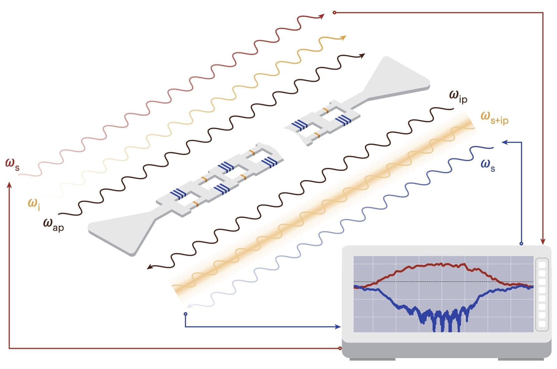
Diffraction-before-destruction of ultrashort X-ray pulses can visualize non-equilibrium processes at the nanoscale with sub-femtosecond precision. Here, the authors demonstrate how the brightness and the spatial resolution of such snapshots can be substantially increased despite ionization.

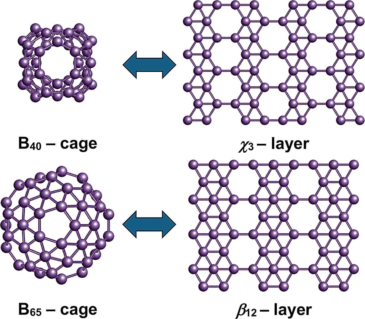
Explore the groundbreaking potential of borophene, a two-dimensional nanomaterial made of boron that outperforms graphene in strength and flexibility. Discover its exceptional properties, including superior electrical and thermal conductivity, unmatched mechanical resistance, and remarkable chemical reactivity. This episode delves into its promising applications in fields such as flexible electronics, energy storage, and nanomedicine. We also compare borophene to graphene and discuss the challenges of scaling up production for widespread use. A deep dive into the material poised to redefine the future of technology.

Novel magnetic nanodiscs could provide a much less invasive way of stimulating parts of the brain, paving the way for stimulation therapies without implants or genetic modification, MIT researchers report.

The scientists envision that the tiny discs, which are about 250 nanometers across (about 1/500 the width of a human hair), would be injected directly into the desired location in the brain. From there, they could be activated at any time simply by applying a magnetic field outside the body. The new particles could quickly find applications in biomedical research, and eventually, after sufficient testing, might be applied to clinical uses.

The development of these nanoparticles is described in the journal Nature Nanotechnology, in a paper by Polina Anikeeva, a professor in MIT’s departments of Materials Science and Engineering and Brain and Cognitive Sciences, graduate student Ye Ji Kim, and 17 others at MIT and in Germany.

Bright, twisted light can be produced with technology similar to an Edison light bulb, researchers at the University of Michigan have shown. The finding adds nuance to fundamental physics while offering a new avenue for robotic vision systems and other applications for light that traces out a helix in space.

“It’s hard to generate enough brightness when producing twisted light with traditional ways like electron or photon luminescence,” said Jun Lu, an adjunct research investigator in chemical engineering at U-M and first author of the study on the cover of this week’s Science.

“We gradually noticed that we actually have a very old way to generate these photons—not relying on photon and electron excitations, but like the bulb Edison developed.”