Menu

Blog

Archive for the ‘materials’ category: Page 125

Jun 27, 2022

Long-hypothesized ‘next generation wonder material’ created for first time

Posted by in category: materials

For over a decade, scientists have attempted to synthesize a new form of carbon called graphyne with limited success. That endeavor is now at an end, though, thanks to new research from the University of Colorado Boulder.

Jun 27, 2022

FINALLY! A Graphene Battery That Could Change Everything | Answers With Joe

Posted by in categories: materials, mobile phones

Get a year of Nebula and Curiosity Stream for only $14.79 when you sign up at http://www.curiositystream.com/joescott.
We’ve been hearing about the potential of graphene for decades, and yet very few of the big promises have come to pass. But a new aluminum graphene battery design is coming out this year that could charge a phone in less than a minute, and it may be the future of energy storage.

Want to support the channel? Here’s how:

Continue reading “FINALLY! A Graphene Battery That Could Change Everything | Answers With Joe” »

Jun 25, 2022

These rechargeable batteries are more sustainable and safer than lithium—and half the cost

Posted by in categories: materials, sustainability

Jun 23, 2022

New Photonic Materials Could Enable Ultra-Fast Light-Based Computing

Posted by in categories: computing, materials

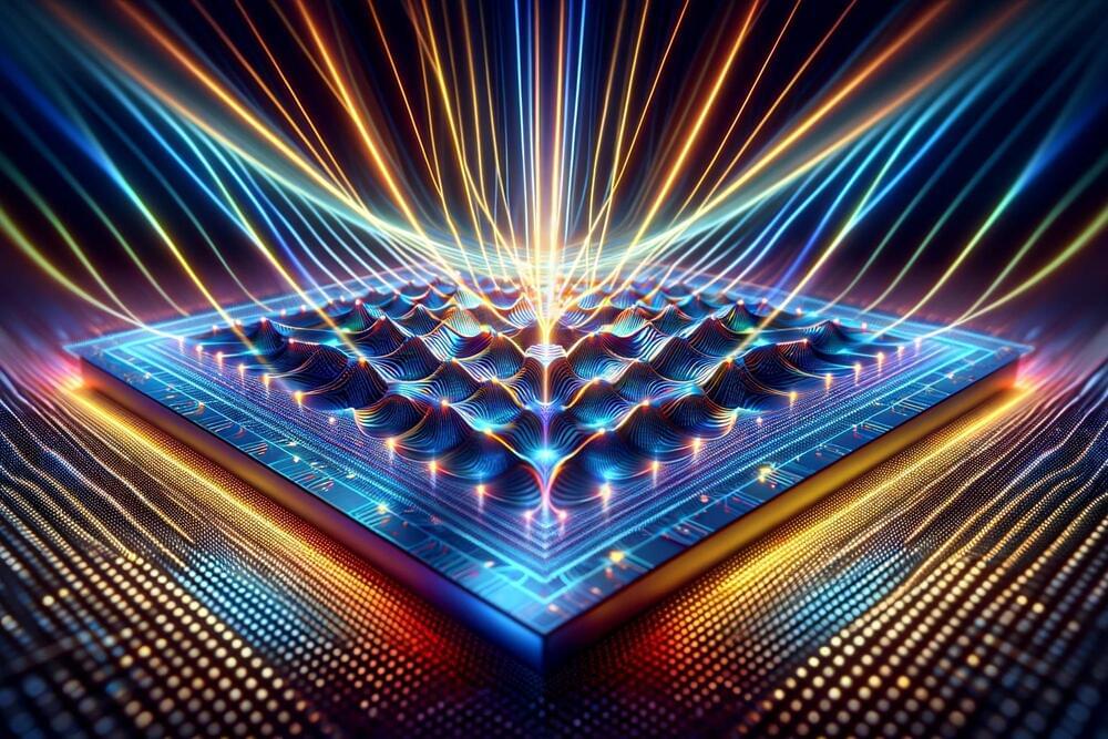
Researchers at the University of Central Florida are developing new photonic materials which may one day be used to enable ultra-fast, low-power light-based computing. The unique materials referred to as topological insulators, resemble wires that have been flipped inside out, with the insulation on the inside and the current flowing along the exterior.

In order to avoid the overheating issue that today’s ever-smaller circuits encounter, topological insulators could be incorporated into circuit designs to enable the packing of more processing power into a given area without generating heat.

The researchers’ most recent study, which was published on April 28 in the journal Nature Materials, presented a brand-new process for creating the materials that make use of a unique, chained honeycomb lattice structure. The linked, honeycombed pattern was laser etched onto a piece of silica, a material often used to create photonic circuits, by the researchers.

Jun 22, 2022

Nvidia’s New AI Model can Convert still Images to 3D Graphics

Posted by in categories: materials, robotics/AI

View insights.


Nvidia has made another attempt to add depth to shallow graphics. After converting 2D images into 3D scenes, models, and videos, the company has turned its focus to editing. The GPU giant today unveiled a new AI method that transforms still photos into 3D objects that creators can modify with ease. Nvidia researchers have developed a new inverse rendering pipeline, Nvidia 3D MoMa that allows users to reconstruct a series of still photos into a 3D computer model of an object, or even a scene. The key benefit of this workflow, compared to more traditional photogrammetry methods, is its ability to output clean 3D models capable of being imported and edited out-of-the-box by 3D gaming and visual engines.

According to reports, other photogrammetry programs will turn 2D images into 3D models, Nvidia’s 3D MoMa technology takes it a step further by producing mesh, material, and lighting information of the subjects and outputting it in a format that’s compatible with existing 3D graphics engines and modeling tools. And it’s all done in a relatively short timeframe, with Nvidia saying 3D MoMa can generate triangle mesh models within an hour using a single Nvidia Tensor Core GPU.

Continue reading “Nvidia’s New AI Model can Convert still Images to 3D Graphics” »

Jun 21, 2022

Deadly snake venom could stop uncontrolled bleeding

Posted by in categories: biotech/medical, materials

Researchers working with snake venom have developed a gel that can stop bleeding. The material solidifies at body temperature to seal wounds.

Jun 20, 2022

We Could Be Close To Controlling Metamaterials With Our Minds

Posted by in category: materials

You can essentially bend light with your mind using the new technology.

Jun 18, 2022

Scientists serendipitously discover rare cluster compound

Posted by in categories: biotech/medical, materials

Scientists at Kyoto University’s Institute for Cell-Material Sciences have discovered a novel cluster compound that could prove useful as a catalyst. Compounds, called polyoxometalates, that contain a large metal-oxide cluster carry a negative charge. They are found everywhere, from anti-viral medicines to rechargeable batteries and flash memory devices.

The new cluster compound is a hydroxy-iodide (HSbOI) and is unusual, as it has large, positively charged clusters. Only a handful of such positively charged cluster compounds have been found and studied.

“In , the discovery of or molecule can create a new science,” says Kyoto University chemist Hiroshi Kageyama. “I believe that these new positively charged clusters have great potential.”

Jun 17, 2022

Did supernovae help form Barnard’s Loop?

Posted by in categories: cosmology, materials

Astronomers studying the structure of the Milky Way galaxy have released the highest-resolution 3D view of the Orion star-forming region. The image and interactive figure were presented today at a press conference hosted by the American Astronomical Society.

Led by researchers at the Center for Astrophysics | Harvard & Smithsonian, the work connects 3D data on young stars and interstellar gas around the Orion complex of star-forming regions. Analysis of the 2D and 3D images, alongside theoretical modeling, shows that supernova explosions within the last 4 million years produced large cavities in the interstellar material associated with Orion.

Continue reading “Did supernovae help form Barnard’s Loop?” »

Jun 16, 2022

Automating semiconductor research with machine learning

Posted by in categories: materials, robotics/AI

The semiconductor industry has been growing steadily ever since its first steps in the mid-twentieth century and, thanks to the high-speed information and communication technologies it enabled, it has given way to the rapid digitalization of society. Today, in line with a tight global energy demand, there is a growing need for faster, more integrated, and more energy-efficient semiconductor devices.

However, modern semiconductor processes have already reached the nanometer scale, and the design of novel high-performance materials now involves the structural analysis of semiconductor nanofilms. Reflection high-energy electron diffraction (RHEED) is a widely used analytical method for this purpose. RHEED can be used to determine the structures that form on the surface of thin films at the atomic level and can even capture structural changes in real time as the thin film is being synthesized!

Unfortunately, for all its benefits, RHEED is sometimes hindered by the fact that its output patterns are complex and difficult to interpret. In virtually all cases, a highly skilled experimenter is needed to make sense of the huge amounts of data that RHEED can produce in the form of diffraction patterns. But what if we could make machine learning do most of the work when processing RHEED data?