Menu

Blog

Archive for the ‘materials’ category: Page 121

Aug 14, 2022

Hubble Space Telescope captures stunning close-up of Orion Nebula

Posted by in categories: materials, space

One of the most beautiful and spectacular parts of the night sky is the Orion constellation.

Herbig-Haro object HH 505 is around 1,000 light-years from the Earth. HH objects are bright patches of nebulosity associated with newborn stars. The photograph was created with 520 ACS images in five different colors to get the sharpest view ever. The Hubble telescope has taken a new magical image of the Orion Nebula.

One of the most beautiful and spectacular parts of the night sky is the Orion constellation. The Orion Nebula is one of the Milky Way’s most studied and photographed objects and a nest of material where young stars are being formed. Alnitak, Saif, and Rigel are floating in a large, dense cloud of interstellar dust and gas between the stars.

Continue reading “Hubble Space Telescope captures stunning close-up of Orion Nebula” »

Aug 12, 2022

For the First, 3D Printed Materials can Sense their Movement

Posted by in categories: 3D printing, materials

3D printed material:

MIT researchers manufactured objects made of flexible plastic and electrically conductive filaments. Some varieties of 3D-printed objects can now feel, using a new technique that builds sensors directly into their materials. 3D printing can be considered printing, although not as it’s traditionally been defined. The method opens opportunities for embedding sensors within architected materials, a class of materials whose mechanical properties are programmed through form and composition.

The researchers also created 3D editing software, known as MetaSense, to help users build interactive devices using these metamaterials. The new technique 3D-prints objects made from metamaterial substances made of grids of repeating cells. It was designed to conform to a person’s hand. When a user squeezes one of the flexible buttons, the resulting electric signals help control a digital synthesizer.

Aug 11, 2022

New programmable 3D printed materials can sense their own movements

Posted by in categories: 3D printing, materials

MIT researchers have developed a method for 3D printing materials with tunable mechanical properties, that sense how they are moving and interacting with the environment. The researchers create these sensing structures using just one material and a single run on a 3D printer.

To accomplish this, the researchers began with 3D-printed lattice materials and incorporated networks of air-filled channels into the structure during the printing process. By measuring how the pressure changes within these channels when the structure is squeezed, bent, or stretched, engineers can receive feedback on how the material is moving.

The method opens opportunities for embedding sensors within architected materials, a class of materials whose mechanical properties are programmed through form and composition. Controlling the geometry of features in architected materials alters their mechanical properties, such as stiffness or toughness. For instance, in cellular structures like the lattices the researchers print, a denser network of cells makes a stiffer structure.

Aug 10, 2022

This oddly-shaped Finnish cabin was made with cross-laminated timber to withstand subarctic cold!

Posted by in categories: materials, sustainability

This cabin in the woods is an otherworldly, all-black, geometric structure built to provide cozy refuge even in harsh Finnish winters. It was designed for a California-based CEO who returned home to Finland with her family to be closer to her ancestral land so she could maintain it. The cabin is aptly named Meteorite based on its unique shape and is set in a clearing surrounded by spruce and birch trees. The cabin is made entirely from cross-laminated timber (CLT) which is a sustainable alternative to other construction materials.

Aug 9, 2022

Transient microelectromechanical systems that can self-dissolve over time

Posted by in categories: futurism, materials

Typically, the key goal of electronics engineers is to develop components and devices that are durable and can operate for long periods of time without being damaged. Such devices require resistant materials, which ultimately contribute to the accumulation of electronic waste on our planet.

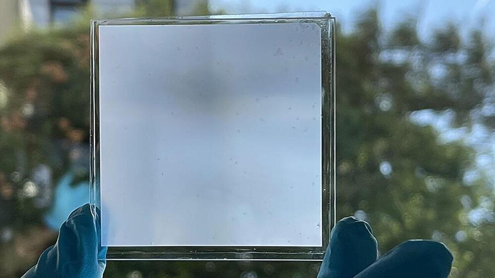
Researchers at Northwestern University and the University of Illinois have been conducting research focusing on an entirely different type of electromechanical system (MEMS): those based on so-called “transient materials.” Transient materials are materials that can dissolve, resorb, disintegrate or physically disappear in other ways at programmed and specific times.

Their most recent paper, published in Nature Electronics, introduces new MEMS based on fully water-soluble materials that could dissolve in their surrounding environment after set periods of time. In the future, these materials could help to decrease the amount of electronic waste, enabling the development of some electronic devices that spontaneously disappear when they are no longer needed.

Aug 9, 2022

Artificial finger able to identify surface material with 90% accuracy

Posted by in categories: materials, robotics/AI

A team of researchers at the Chinese Academy of Sciences, has developed an artificial finger that was able to identify certain surface materials with 90% accuracy. In their paper published in the journal Science Advances, the group describes how they used triboelectric sensors to give their test finger an ability to gain a sense of touch.

Prior research has led to the development of robotic fingers that have the ability to recognize certain attributes of certain surfaces, such as or temperature—the team with this new effort, have taken such efforts further by adding the ability to identify a material that is being touched.

Continue reading “Artificial finger able to identify surface material with 90% accuracy” »

Aug 7, 2022

Is there anything green about plastic grass?

Posted by in category: materials

More people are swapping real lawns for fake but experts are worried about its environmental impact.

Aug 7, 2022

Self-stabilizing photonic levitation and propulsion of nanostructured macroscopic objects

Posted by in categories: materials, nanotechnology

Circa 2019


Mechanical stability of macroscopic structures on the millimetre-, centimetre-and even metre-scale could be realized by tailoring the anisotropy of light scattering along the object’s surface, without needing to focus incident light or excessively constrain the shape, size or material composition of the object.

Aug 6, 2022

Semiconductors in the Spotlight

Posted by in categories: electronics, materials

A new model suggests that lattice defects are responsible for the way some semiconductors become harder under illumination.

Understanding how semiconductors respond to illumination has been crucial to the development of photovoltaics and optical sensors. But some light-induced behaviors have been less thoroughly investigated. For example, when some semiconductors are illuminated, their mechanical properties can change drastically, a phenomenon known as photoelasticity. Photoelastic materials could be useful in the development of flexible electronics, but researchers do not understand in detail the mechanism behind the effect. Now, based on experiments and simulations, Rafael Jaramillo of the Massachusetts Institute of Technology and colleagues present a new theoretical framework that explains photoelasticity in terms of lattice defects [1].

The researchers used a diamond-tipped probe to make nanometer-scale indentations in samples of zinc oxide, zinc sulfide, and cadmium sulfide—first in the dark, and then under a range of visible and ultraviolet wavelengths. All three materials hardened to varying degrees when illuminated, with cadmium sulfide showing the largest and most consistent response. For every sample, the effect increased as the photon energy increased toward the material’s band gap.

Aug 3, 2022

Nendo stacks concrete tunnels to create archive and guesthouse in Miyota

Posted by in category: materials

Japanese studio Nendo has created an archive to house its products and furniture from precast concrete box culverts in central Japan.

Named Culvert Guesthouse, the archive and residence was constructed from four tunnel-like forms that were stacked on top of each other.

Designed by the studio as its own archive, the distinctive-shaped building is located in dense woodland on the edge of the town of Miyota in Nagano Prefecture.