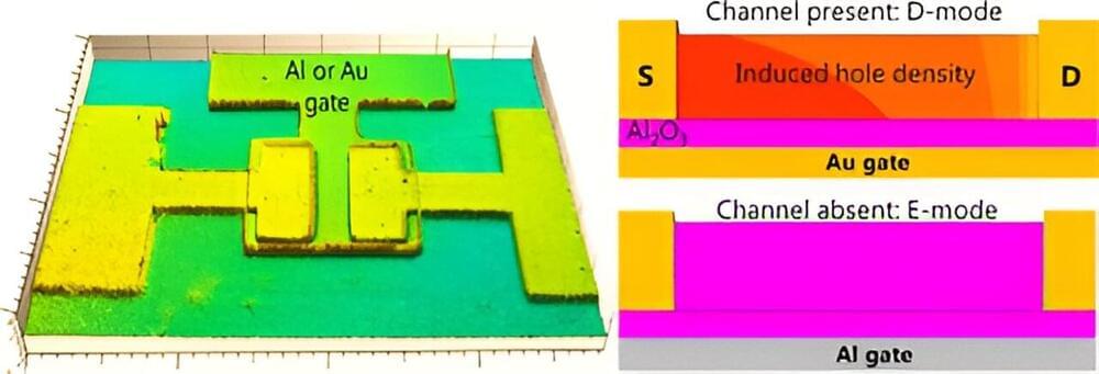
Nanoscale transistors are in demand for efficient digital circuits, and biasing of each device is critical. These stringent biasing conditions can be relaxed by obtaining precise values of the threshold voltages of the transistor. This leads to more tolerant logic states to the electrical noise.
To meet the requirements of reduced power consumption, CMOS field-effect transistors (FETs) are fabricated such that they operate in enhancement (E) mode, i.e., there are no free charge carriers in the channel at zero gate voltage. On the other hand, depletion (D) mode transistors have higher currents than enhancement mode due to ample charge carrier density.
In contrast to switching applications of FET, for high-frequency applications, off-state of FET is not a compulsory requirement. In fact, the presence of a channel at zero gate bias is advantageous to obtain high transconductance at lower voltages. For Si FETs, the enhancement or depletion modes were determined at the fabrication step of ion implantation doping. However, it is challenging to implement this solution for the new generation of thin materials like organic semiconductors and 2D materials.
