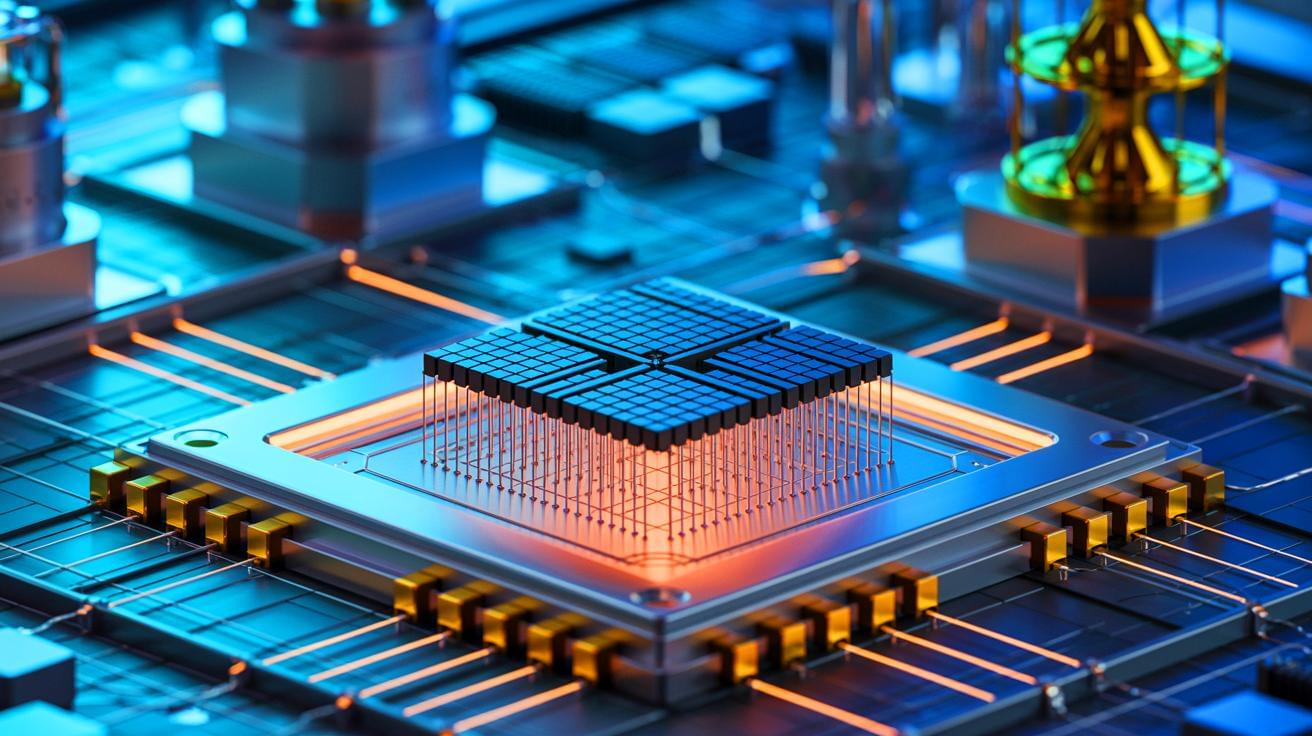
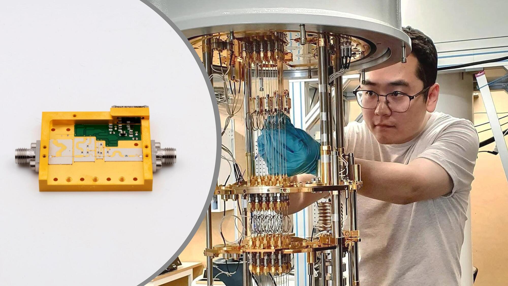
Toggle light / dark theme

Time interfaces: The gateway to four-dimensional quantum optics

A new study from the University of Eastern Finland (UEF) explores the behavior of photons, the elementary particles of light, as they encounter boundaries where material properties change rapidly over time. This research uncovers remarkable quantum optical phenomena that may enhance quantum technology and paves the road for an exciting nascent field: four-dimensional quantum optics.

Four-dimensional optics is a research area investigating light scattering from structures which change in time and space. It holds immense promise for advancing microwave and optical technologies by enabling functionalities such as frequency conversion, amplification, polarization engineering and asymmetric scattering. That is why it has captured the interest of many researchers across the globe.

Previous years have seen significant strides in this area. For instance, a 2024 study published in Nature Photonics and also involving UEF highlights how incorporating optical features like resonances can drastically influence the interaction of electromagnetic fields with time-varying two-dimensional structures, opening exotic possibilities to control light.

Quantum fractal patterns visualized

A team of scientists from Princeton University has measured the energies of electrons in a new class of quantum materials and has found them to follow a fractal pattern. Fractals are self-repeating patterns that occur on different length scales and can be seen in nature in a variety of settings, including snowflakes, ferns, and coastlines.

A quantum version of a , known as “Hofstadter’s butterfly,” has long been predicted, but the new study marks the first time it has been directly observed experimentally in a real material. This research paves the way toward understanding how interactions among electrons, which were left out of the theory originally proposed in 1976, give rise to new features in these quantum fractals.

The study was made possible by a recent breakthrough in , which involved stacking and twisting two sheets of carbon atoms to create a pattern of electrons that resembles a common French textile known as a moiré design.

PsiQuantum Announces Omega, a Manufacturable Chipset for Photonic Quantum Computing

PsiQuantum unveiled Omega, a quantum photonic chipset designed for large-scale quantum computing. This development, detailed in a Nature publication, marks a significant milestone in the mass production of quantum chips. Manufactured in partnership with GlobalFoundries at their Albany, New York facility, Omega integrates advanced components essential for constructing million-qubit quantum computers. The chipset employs photonics technology, manipulating single photons for computations, which offers advantages such as simplified cooling mechanisms. PsiQuantum has achieved manufacturing yields comparable to standard semiconductors, producing millions of these chips. The company plans to establish two Quantum Compute Centers in Brisbane, Australia, and Chicago, Illinois, aiming for operational facilities by 2027. This progress positions PsiQuantum at the forefront of the quantum computing industry, alongside other major companies making significant strides in the field. Summary of the paper in Nature: For decades, scientists have dreamed of building powerful quantum computers using light—photonic quantum computers. These machines could solve complex problems far beyond the reach of today’s most advanced supercomputers. However, a major roadblock has been the sheer difficulty of manufacturing the components required at the necessary scale. Now, researchers have developed a manufacturable platform for photonic quantum computing, marking a significant breakthrough. Their system is built using silicon photonics, a technology that integrates optical components directly onto a chip, much like modern semiconductor chips. The team demonstrated key capabilities: * Ultra-precise qubits: They achieved a stunning 99.98% accuracy in preparing and measuring quantum states. * Reliable quantum interference: Independent photon sources interacted with a visibility of 99.50%, crucial for quantum logic operations. * High-fidelity entanglement: A critical quantum process, known as two-qubit fusion, reached 99.22% accuracy. * Seamless chip-to-chip connections: The team linked quantum chips with 99.72% fidelity, a crucial step for scaling up quantum systems. Looking ahead, the researchers highlight new technologies that will further improve performance, including better photon sources, advanced detectors, and high-speed switches. This work represents a major step toward large-scale, practical quantum computing, bringing us closer to a future where quantum machines tackle problems that are impossible today.


PsiQuantum’s focus is now on wiring these chips together across racks, into increasingly large-scale multi-chip systems – work the company is now expanding through its partnership with the U.S. Department of Energy at SLAC National Accelerator Laboratory in Menlo Park, California as well as a new manufacturing and testing facility in Silicon Valley. While chip-to-chip networking remains a hard research problem for many other approaches, photonic quantum computers have the intrinsic advantage that photonic qubits can be networked using standard telecom optical fiber without any conversion between modalities, and PsiQuantum has already demonstrated high-fidelity quantum interconnects over distances up to 250m.

In 2024, PsiQuantum announced two landmark partnerships with the Australian Federal and Queensland State governments, as well as the State of Illinois and the City of Chicago, to build its first utility-scale quantum computers in Brisbane and Chicago. Recognizing quantum as a sovereign capability, these partnerships underscore the urgency and race towards building million-qubit systems. Later this year, PsiQuantum will break ground on Quantum Compute Centers at both sites, where the first utility-scale, million-qubit systems will be deployed.

China hits quantum internet record with 2.38 kbps speed over 65 miles

Chinese researchers have allegedly made a major breakthrough in Quantum Secure Direct Communication (QSDC). According to reports, the team has developed a new communication protocol that allows secure data transmission using quantum mechanics principles, setting a world record for transmission speed and distance.

In case you are unaware, QSDC is a type of quantum communication that directly transmits information in quantum states (such as photons) without needing encryption keys like traditional methods (e.g., quantum key distribution or QKD).

Research illuminates the path to superior electro-optic performance in aluminum scandium nitride alloys

From integrated photonics to quantum information science, the ability to control light with electric fields—a phenomenon known as the electro-optic effect—supports vital applications such as light modulation and frequency transduction. These components rely on nonlinear optical materials, in which light waves can be manipulated by applying electric fields.

Conventional nonlinear optical materials such as lithium niobate have a large electro-optic response but are hard to integrate with silicon devices. In the search for silicon-compatible materials, aluminum scandium nitride (AlScN), which had already been flagged as an excellent piezoelectric—referring to a material’s ability to generate electricity when pressure is applied, or to deform when an electric field is applied—has come to the fore. However, better control of its properties and means to enhance its electro-optic coefficients are still required.

Researchers in Chris Van de Walle’s computational materials group at UC Santa Barbara have now uncovered ways to achieve these goals. Their study, published in Applied Physics Letters, explains how adjusting the material’s atomic structure and composition can boost its performance. Strong electro-optic response requires a large concentration of scandium—but the specific arrangement of the scandium atoms within the AlN crystal lattice matters.

Mesoporous silicon: Etching technique reveals unique electronic transport properties

Silicon is the best-known semiconductor material. However, controlled nanostructuring drastically alters the material’s properties. Using a specially developed etching apparatus, a team at HZB has now produced mesoporous silicon layers with countless tiny pores and investigated their electrical and thermal conductivity.

For the first time, the researchers elucidated the electronic transport mechanism in this mesoporous silicon. The material has great potential for applications and could also be used to thermally insulate qubits for quantum computers. The work is published in Small Structures.

Mesoporous silicon is with disordered nanometer-sized pores. The material has a huge internal surface area and is also biocompatible. This opens up a wide range of potential applications, from biosensors to battery anodes and capacitors. In addition, the material’s exceptionally low thermal conductivity suggests applications as thermal insulator.

Engineers show industrial potential of diamond quantum sensors for EV battery monitoring

Researchers at the Technical University of Munich (TUM) have invented an entirely new field of microscopy called nuclear spin microscopy. The team can visualize magnetic signals of nuclear magnetic resonance with a microscope. Quantum sensors convert the signals into light, enabling extremely high-resolution optical imaging.

Magnetic resonance imaging (MRI) scanners are known for their ability to look deep into the human body and create images of organs and tissues. The new method, published in the journal Nature Communications, extends this technique to the realm of microscopic detail.

“The used make it possible to convert signals into optical signals. These signals are captured by a camera and displayed as images,” explains Dominik Bucher, Professor of Quantum Sensing and researcher at the Cluster of Excellence Munich Center for Quantum Science and Technology (MCQST).

/* */