Korean scientists claim their particle-removing oil-coated filter (PRO) captures significantly more particles and is effective over twice as long as a traditional filter.



Two independent groups optimize diamond-based quantum sensing by using more than 100 such sensors in parallel.
Diamond has long been prized for its beauty, and it holds the record as the hardest known natural material. By introducing nitrogen atoms into its crystal lattice, it can also be transformed into a remarkable quantum sensor. The associated crystal defects are known as nitrogen-vacancy (NV) centers, and they imbue such sensors with unprecedented electromagnetic-field sensitivity and excellent spatial resolution [1]. However, experimental platforms designed to exploit these sensors have so far had limited applicability because the sensing speed and resolution are difficult to simultaneously optimize. Now two research teams—one led by Shimon Kolkowitz at the University of California, Berkeley, [2] and the other by Nathalie de Leon at Princeton University [3]—have independently developed a way of manipulating and measuring more than 100 NV centers in parallel (Fig. 1).
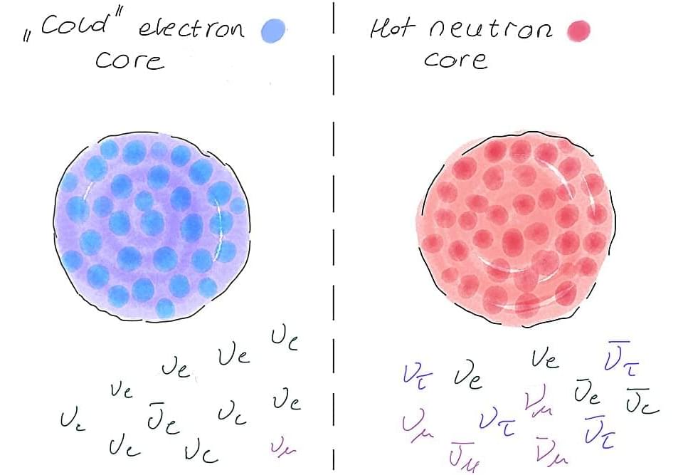
Neutrinos are cosmic tricksters, paradoxically hardly there but lethal to stars significantly more massive than the sun.
These elementary particles come in three known “flavors”: electron, muon and tau. Whatever the flavor, neutrinos are notoriously slippery, and much about their properties remains mysterious. It is almost impossible to collide neutrinos with each other in the lab, so it is not known if neutrinos interact with each other according to the standard model of particle physics, or if there are much-speculated “secret” interactions only among neutrinos.
Now a team of researchers from the Network for Neutrinos, Nuclear Astrophysics, and Symmetries (N3AS), including several from UC San Diego, have shown, through theoretical calculations, how collapsing massive stars can act as a “neutrino collider.” Neutrinos steal thermal energy from these stars, forcing them to contract and causing their electrons to move near light speed. This drives the stars to instability and collapse.

For nearly a century, scientists around the world have been searching for dark matter—an invisible substance believed to make up about 80% of the universe’s mass and needed to explain a variety of physical phenomena. Numerous methods have been used in attempts to detect dark matter, from trying to produce it in particle accelerators to searching for cosmic radiation that it might emit in space.
Yet even today, very little is known about this matter’s fundamental properties. Although it operates in the background, dark matter is believed to influence visible matter, but in ways so subtle that they currently cannot be directly measured.
Scientists believe that if a nuclear clock is developed—one that uses the atomic nucleus to measure time with extreme precision —even the tiniest irregularities in its ticking could reveal dark matter’s influence. Last year, physicists in Germany and Colorado made a breakthrough toward building such a clock, using the radioactive element thorium-229.
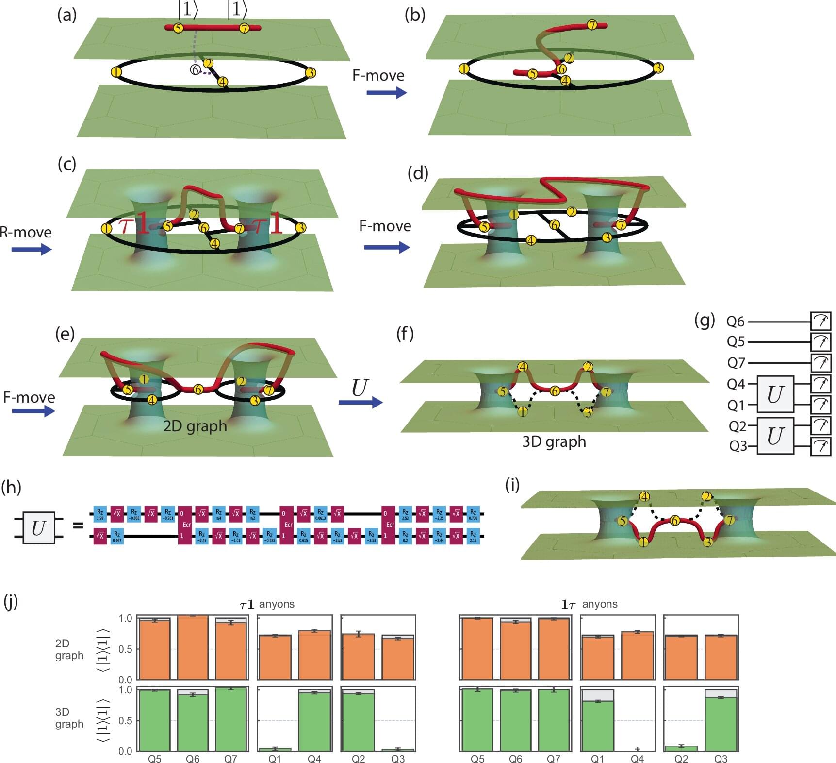
The quantum computing revolution draws ever nearer, but the need for a computer that makes correctable errors continues to hold it back.
Through a collaboration with IBM led by Cornell, researchers have brought that revolution one step closer, achieving two major breakthroughs. First, they demonstrated an error-resistant implementation of universal quantum gates, the essential building blocks of quantum computation. Second, they showcased the power of a topological quantum computer in solving hard problems that a conventional computer couldn’t manage.
In the article “Realizing String-Net Condensation: Fibonacci Anyon Braiding for Universal Gates and Sampling Chromatic Polynomials” published in Nature Communications, an international collaboration between researchers at IBM, Cornell, Harvard University and the Weizman Institute of Science demonstrated, for the first time, the ability to encode information by braiding—moving in a particular order—Fibonacci string net condensate (Fib SNC) anyons, which are exotic quasi-particles, in two dimensional space.

A powerful new method to control magnetic behavior in ultra-thin materials could lead to faster, smaller and more energy-efficient technologies, a study suggests.
Researchers have developed a new way to precisely tune magnetism using a material—called CrPS4—that is just a few atoms thick. The study is published in the journal Nature Materials.
The advance could solve a long-standing scientific problem and pave the way for the development of new smart magnetic technologies, from computer memory devices to next-generation electronics, the team says.

Spintronics are promising devices that work utilizing not only the charge of electrons, like conventional electronics, but also their spin (i.e., their intrinsic angular momentum). The development of fast and energy-efficient spintronic devices greatly depends on the identification of materials with a tunable spin-selective conductivity, which essentially means that engineers can control how electrons with different spin orientations move through these materials, ideally using external magnetic or electric fields.

When Einstein’s predicted ripples in spacetime pass through magnetic fields, they cause the current carrying wires to dance at the gravitational wave frequency, creating potentially detectable electrical signals. Researchers have discovered that the same powerful magnets used to hunt for dark matter could double as gravitational wave detectors. This means experiments already searching for the universe’s most elusive particles could simultaneously capture collisions between black holes and neutron stars, getting two of physics’ most ambitious experiments for the price of one, while potentially opening entirely new windows into the universe’s most violent events.
Dark matter is one of nature’s most confounding mysteries. It keeps particle physicists up at night and cosmologists glued to their supercomputer simulations. We know it’s real because its mass prevents galaxies from falling apart. But we don’t know what it is.
Dark matter doesn’t like other matter and may prefer its own company. While it doesn’t seem to interact with regular baryonic matter, it could possibly react with itself and self-annihilate. It needs a tightly-packed environment to do that, and that may lead to a way astrophysicists can finally detect it.
New theoretical research outlines how this could happen and states that sub-stellar objects, basically brown dwarfs, could host the process. The research is titled “Dark dwarfs: dark matter-powered sub-stellar objects awaiting discovery at the galactic center,” and it’s published in the Journal of Cosmology and Astroparticle Physics. The lead author is Djuna Croon, a theoretical physicist and assistant professor in the Institute for Particle Physics Phenomenology in the Department of Physics at Durham University.

The official Periodic Table of the Elements is one step closer to adding element 117 to its ranks. That’s thanks to an international team of scientists that was able to successfully create several atoms of element 117, which is currently known as Ununseptium until it’s given an official name.
The paper for this experiment has been published in Physical Review Letters.
Element 117 was first created in a joint collaboration between American and Russian scientists back in 2010. However, before an element can be officially added to the Periodic Table of Elements, its discovery must be independently confirmed.