Get a Wonderful Person Tee: https://teespring.com/stores/whatdamath.
More cool designs are on Amazon: https://amzn.to/3QFIrFX
Alternatively, PayPal donations can be sent here: http://paypal.me/whatdamath.
Hello and welcome! My name is Anton and in this video, we will talk about new discoveries about bacterial communication.
Links:
https://www.science.org/doi/10.1126/sciadv.adj1539
https://www.lboro.ac.uk/news-events/news/2025/january/cyanob…formation/
https://en.wikipedia.org/wiki/Prochlorococcus.
Previous video:
#biology #bacteria #biofilm.
0:00 Bacterial communication.
0:35 Cyanobacteria complexity.
3:00 Most prominent bacterium in the ocean.
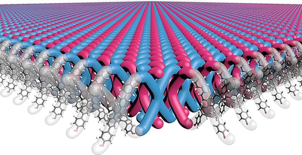
4:10 Bizarre discoveries of nanotubes.
5:25 Possible explanations and studies trying to figure it out.
6:15 Recent study finds interspecies communication.
8:10 Entirely new way to communicate or a trade network?
9:30 Questions and future studies.
10:50 Conclusions.
Support this channel on Patreon to help me make this a full time job:
https://www.patreon.com/whatdamath.
Bitcoin/Ethereum to spare? Donate them here to help this channel grow!
bc1qnkl3nk0zt7w0xzrgur9pnkcduj7a3xxllcn7d4
or ETH: 0x60f088B10b03115405d313f964BeA93eF0Bd3DbF
Space Engine is available for free here: http://spaceengine.org.