+ Decoding the secrets of DNA, CRISPR gene editing allows scientists to target specific genes linked to aging. By modifying these genes, researchers aim to prevent conditions that come with aging. Envision a future where genetic risks for age-related diseases are minimized through precise DNA editing.
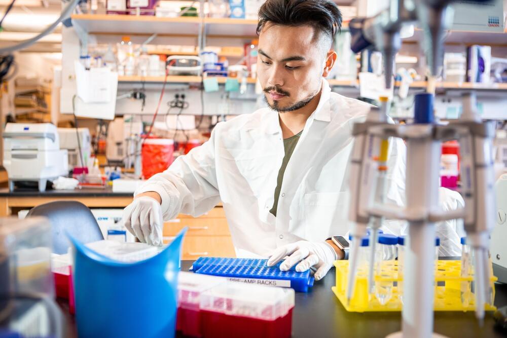
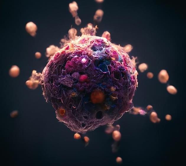
It is possible to regenerate cells using stem cells, which can turn into a variety of types. In recent trials, stem cells showed promise in regenerating aged tissues like cartilage. Scientists hope to develop therapies that might slow down physical decline and maintain vitality longer by using this potential.
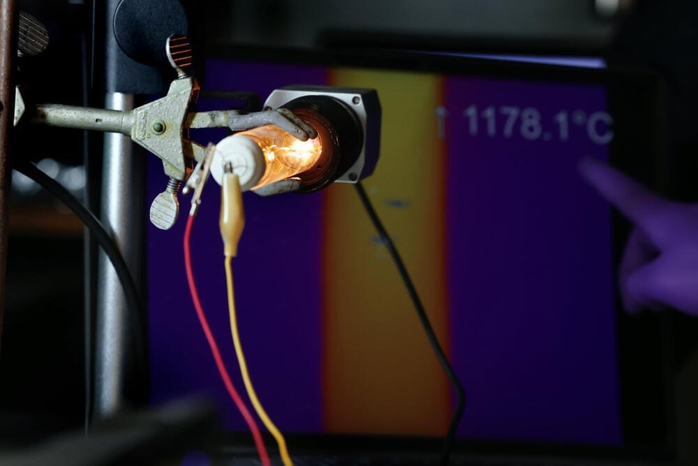
Nanobots could someday be the future of healthcare by targeting damaged cells directly as they move through your bloodstream. Researchers are currently exploring how nanobots might repair cellular damage and improve overall health, potentially reversing some age-related effects at the cellular level.
As the protective ends of chromosomes, telomeres shorten over time. When they become too short, cells stop functioning. In laboratory studies, researchers have extended the lifespan of animals by using telomere extension techniques. Though still experimental, this research could pave the way for human applications in slowing aging.
Do you agree with this list?
Advances in human longevity are no longer science fiction. Groundbreaking discoveries in fields like genetics, nanotechnology, and regenerative medicine are unlocking the secrets of aging. These 20 developments highlight how science is changing our understanding of what it means to grow older.