Middlemen get a bad rap for adding cost and complications to an operation. So, eliminating the go-betweens can reduce expense and simplify a process, increasing efficiency and consumer happiness.
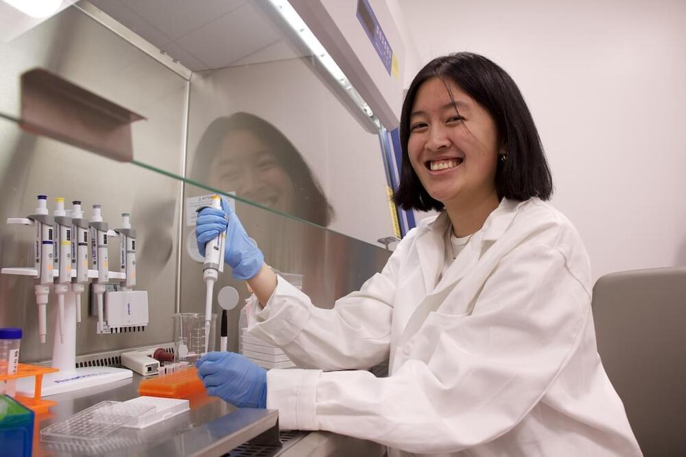
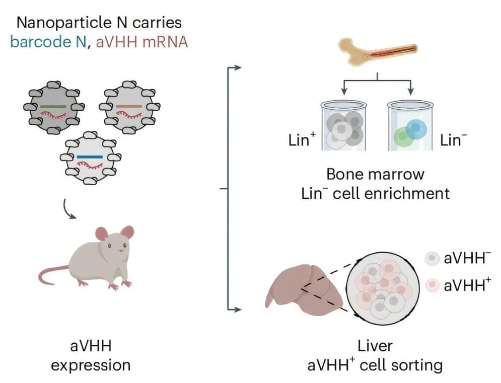
James Dahlman and his research team have been thinking along those same lines for stem cell treatments. They’ve created a technique that eliminates noisome middlemen and could lead to new, less-invasive treatments for blood disorders and genetic diseases. It sidesteps the discomfort and risks of current treatments, making life easier for patients.
“This would be an alternative to invasive hematopoietic stem cell therapies—we could just give you an IV drip,” said Dahlman, McCamish Early Career Professor in the Wallace H. Coulter Department of Biomedical Engineering. “It simplifies the process and reduces the risks to patients. That’s why this work is important.”