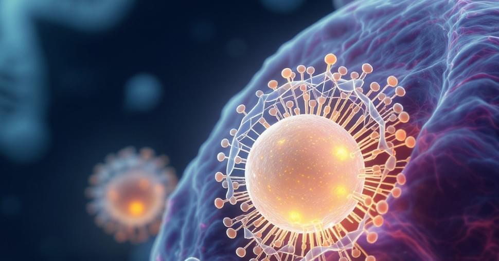
Menu

Blog

Archive for the ‘nanotechnology’ category: Page 3

Jun 16, 2024

Self-assembling and disassembling swarm molecular robots via DNA molecular controller

Posted by in categories: biotech/medical, nanotechnology, robotics/AI

Researchers from Tohoku University and Kyoto University have successfully developed a DNA-based molecular controller that autonomously directs the assembly and disassembly of molecular robots. This pioneering technology marks a significant step towards advanced autonomous molecular systems with potential applications in medicine and nanotechnology.

Details of the breakthrough were published in the journal Science Advances (“Autonomous assembly and disassembly of gliding molecular robots regulated by a DNA-based molecular controller”).

“Our newly developed molecular controller, composed of artificially designed DNA molecules and enzymes, coexists with molecular robots and controls them by outputting specific DNA molecules,” points out Shin-ichiro M. Nomura, an associate professor at Tohoku University’s Graduate School of Engineering and co-author of the study. “This allows the molecular robots to self-assemble and disassemble automatically, without the need for external manipulation.”

Jun 15, 2024

Going smaller to gain more

Posted by in categories: nanotechnology, particle physics

Nanotechnology has arrived in the turfgrass industry. What will the presence of tiny particles mean for fertility and plant protectant applications?

Jun 14, 2024

Researchers create nanocubes forming floating checkerboards via self-assembly

Posted by in categories: chemistry, engineering, nanotechnology

Researchers have engineered nanosized cubes that spontaneously form a two-dimensional checkerboard pattern when dropped on the surface of water. The work, published in Nature Communications (“Self-assembly of nanocrystal checkerboard patterns via non-specific interactions”), presents a simple approach to create complex nanostructures through a technique called self-assembly.

“It’s a cool way to get materials to build themselves,” said study co-senior author Andrea Tao, a professor in the Aiiso Yufeng Li Family Department of Chemical and Nano Engineering at the University of California San Diego. “You don’t have to go into a nanofabrication lab and do all these complex and precise manipulations.”

Each nanocube is composed of a silver crystal with a mixture of hydrophobic (oily) and hydrophilic (water-loving) molecules attached to the surface. When a suspension of these nanocubes is introduced to a water surface, they arrange themselves such that they touch at their corner edges. This arrangement creates an alternating pattern of solid cubes and empty spaces, resulting in a checkerboard pattern.

Jun 12, 2024

Quantum dot based metasurface enables two objects to exist in the same space

Posted by in categories: chemistry, engineering, nanotechnology, quantum physics

In relationships, sharing closer spaces naturally deepens the connection as bonds form and strengthen through increasing shared memories. This principle applies not only to human interactions but also to engineering. Recently, an intriguing study was published demonstrating the use of quantum dots to create metasurfaces, enabling two objects to exist in the same space.

Professor Junsuk Rho from the Department of Mechanical Engineering, the Department of Chemical Engineering, and the Department of Electrical Engineering, PhD candidates Minsu Jeong, Byoungsu Ko, and Jaekyung Kim from the Department of Mechanical Engineering, and Chunghwan Jung, a PhD candidate, from the Department of Chemical Engineering at Pohang University of Science and Technology (POSTECH) employed Nanoimprint Lithography (NIL) to fabricate metasurfaces embedded with quantum dots, enhancing their luminescence efficiency. Their research was recently published in Nano Letters (“Printable Light-Emitting Metasurfaces with Enhanced Directional Photoluminescence”).

(Left) Schematic diagram of the fabrication of a luminescence-controlled metasurface using the nanoimprint lithography process. (Right) Experiment evaluating the performance of the metasurface’s luminescence control. (Image: POSTECH)

Jun 12, 2024

Switching nanomagnets using infrared lasers

Posted by in categories: nanotechnology, physics

When molecules are irradiated with infrared light, they begin to vibrate due to the energy supply. For Andreas Hauser from the Institute of Experimental Physics at Graz University of Technology (TU Graz), this well-known phenomenon was the starting point for considering whether these oscillations could also be used to generate magnetic fields.

Jun 11, 2024

A nanomaterial one-two punch quickly heals wounds in diabetic animal model

Posted by in categories: biotech/medical, nanotechnology

Diabetic wounds are slow-healing, potentially life-threatening complications with limited treatment options. But a two-step, nanomaterial-based strategy may open doors to better care.

Jun 11, 2024

A chain of copper and carbon atoms may be the thinnest metallic wire

Posted by in categories: computing, information science, nanotechnology, particle physics

While carbon nanotubes are the materials that have received most of the attention so far, they have proved very difficult to manufacture and control, so scientists are eager to find other compounds that could be used to create nanowires and nanotubes with equally interesting properties, but easier to handle.

So, Chiara Cignarella, Davide Campi and Nicola Marzari thought to use to parse known three-dimensional crystals, looking for those that—based on their structural and —look like they could be easily “exfoliated,” essentially peeling away from them a stable 1-D structure. The same method has been successfully used in the past to study 2D materials, but this is the first application to their 1-D counterparts.

The researchers started from a collection of over 780,000 crystals, taken from various databases found in the literature and held together by van der Waals forces, the sort of weak interactions that happen when atoms are close enough for their electrons to overlap. Then they applied an algorithm that considered the spatial organization of their atoms looking for the ones that incorporated wire-like structures, and calculated how much energy would be necessary to separate that 1-D structure from the rest of the crystal.

Jun 10, 2024

New study reveals brain’s fractal-like structure near phase transition, a finding that may be universal across species

Posted by in categories: nanotechnology, neuroscience, physics

While researchers have long studied brain dynamics using imaging (fMRI) and electroencephalograms (EEG), advances in neuroscience have only recently provided massive datasets for the brain’s cellular structure. These data opened possibilities for Kovács and his team to apply statistical physics techniques to measure the physical structure of neurons.

For the new study, Kovács and Ansell analyzed publicly available data of 3D brain reconstructions from humans, fruit flies and mice. By examining the brain at nanoscale resolution, the researchers found the samples showcased hallmarks of physical properties associated with criticality.

One such property is the well-known, fractal-like structure of neurons. This nontrivial fractal-dimension is an example of a set of observables, called “critical exponents,” that emerge when a system is close to a phase transition.

Jun 9, 2024

Unveiling novel energy phenomena from light exposure on layered materials

Posted by in categories: nanotechnology, particle physics

Research groups from the University of Tsukuba and the University of Rennes have discovered a novel phenomenon in which a nested structure of carbon nanotubes enveloped in boron nitride nanotubes facilitates a unique electron escape route when exposed to light. This finding introduces promising avenues for various applications, including the creation of high-speed optical devices, rapid control of electrons and other particles and efficient heat dissipation from devices.

Jun 9, 2024

NV Centre Quantum Sensors: A New Era In Condensed Matter Physics Study

Posted by in categories: nanotechnology, quantum physics

Researchers from Princeton University, University of California Santa Barbara, University of Basel, and ETH Zurich have discovered new applications for nitrogen vacancy (NV) centre quantum sensors in condensed matter physics. These sensors, which offer nanoscale resolution across a wide range of temperatures, have been used to measure static magnetic fields in condensed matter systems.

NV centres can probe beyond average magnetic fields, enabling high precision noise sensing in diverse systems. They offer several advantages over other nanoscale probes, including the ability to probe both static and dynamic properties in a momentum and frequency-resolved way.

Condensed matter physics is a field that studies the physical properties of condensed phases of matter, such as solids and liquids. Recently, researchers from Princeton University, University of California Santa Barbara, University of Basel, and ETH Zurich have discovered new opportunities in this field for nanoscale quantum sensors, specifically nitrogen vacancy (NV) centre quantum sensors. These sensors offer unique advantages in studying condensed matter systems due to their quantitative, noninvasive, physically robust nature, and their ability to offer nanoscale resolution across a wide range of temperatures.

Page 3 of 28812345678Last