Menu

Blog

Archive for the ‘nanotechnology’ category: Page 273

Jun 6, 2016

Meta-lens works in the visible spectrum, sees smaller than a wavelength of light

Posted by in category: nanotechnology

Curved lenses, like those in cameras or telescopes, are stacked in order to reduce distortions and resolve a clear image. That’s why high-power microscopes are so big and telephoto lenses so long.

While lens technology has come a long way, it is still difficult to make a compact and thin lens (rub a finger over the back of a cellphone and you’ll get a sense of how difficult). But what if you could replace those stacks with a single flat—or planar—lens?

Researchers from the Harvard John A. Paulson School of Engineering and Applied Sciences (SEAS) have demonstrated the first planar lens that works with high efficiency within the of light—covering the whole range of colors from red to blue. The lens can resolve nanoscale features separated by distances smaller than the wavelength of light. It uses an ultrathin array of tiny waveguides, known as a metasurface, which bends light as it passes through, similar to a curved lens.

Continue reading “Meta-lens works in the visible spectrum, sees smaller than a wavelength of light” »

Jun 6, 2016

Applications of Nanoparticle Tracking Analysis in Nanomedicine

Posted by in categories: nanotechnology, quantum physics

Since 2001, I have worked, experimented, and researched in parallel tech and bio/medical technology space. I did this because I could see that at some point that these two fields would eventually overlap and eventually merge in many areas. Today, we’re already see the duplicated use of technology in both the medical/ life sciences and the same technology used to advance the technology in general such as Quantum tech, nanotech, etc. Here is another example of this trend.


Sponsored Content by

Introduction

Continue reading “Applications of Nanoparticle Tracking Analysis in Nanomedicine” »

Jun 6, 2016

Tiny lasers on silicon means big things for electronics

Posted by in categories: computing, electronics, nanotechnology, quantum physics, solar power, sustainability

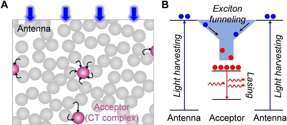
Silicon forms the basis of everything from solar cells to the integrated circuits at the heart of our modern electronic gadgets. However the laser, one of the most ubiquitous of all electronic devices today, has long been one component unable to be successfully replicated in this material. Now researchers have found a way to create microscopically-small lasers directly from silicon, unlocking the possibilities of direct integration of photonics on silicon and taking a significant step towards light-based computers.

Whilst there has been a range of microminiature lasers incorporated directly into silicon over the years, including melding germanium-tin lasers with a silicon substrate and using gallium-arsenide (GaAs) to grow laser nanowires, these methods have involved compromise. With the new method, though, an international team of researchers has integrated sub-wavelength cavities, the basic components of their minuscule lasers, directly onto the silicon itself.

To help achieve this, a team of collaborating scientists from Hong Kong University of Science and Technology, the University of California, Santa Barbara, Sandia National Laboratories and Harvard University, first had to find a way to refine silicon crystal lattices so that their inherent defects were reduced significantly enough to match the smooth properties found in GaAs substrate lasers. They did this by etching nano-patterns directly onto the silicon to confine the defects and ensure the necessary quantum confinement of electrons within quantum dots grown on this template.

Read more

Jun 4, 2016

Flat lens promises possible revolution in optics

Posted by in category: nanotechnology

A flat lens made of paint whitener on a sliver of glass could revolutionise optics, according to its US inventors.

Just 2mm across and finer than a human hair, the tiny device can magnify nanoscale objects and gives a sharper focus than top-end microscope lenses.

It is the latest example of the power of metamaterials, whose novel properties emerge from their structure.

Read more

Jun 2, 2016

Tiny lasers enable next-gen microprocessors to run faster, less power-hungry

Posted by in categories: electronics, energy, nanotechnology

More energy efficient, high performance microprocessors on the way.


Abstract: Tiny high-performance lasers grown directly on silicon wafers solve a decades-old semiconductor industry challenge that, until now, has held back the integration of photonics with electronics on the silicon platform,

A group of scientists from Hong Kong University of Science and Technology; the University of California, Santa Barbara; Sandia National Laboratories and Harvard University were able to fabricate tiny lasers directly on silicon — a huge breakthrough for the semiconductor industry and well beyond.

Continue reading “Tiny lasers enable next-gen microprocessors to run faster, less power-hungry” »

Jun 2, 2016

New nanotech fabric dissolves odor and stains whenever it’s exposed to bright light

Posted by in categories: energy, nanotechnology

Not a big fan of laundry day? Well what if you could wash your clothes just by stepping into the sunshine? Thanks to researchers at RMIT University in Melbourne, a self-cleaning textile could make that possible in the very near future. With the help of special nanostructures grown directly into the fabric, these new textiles could degrade organic matter like dirt, dust, and sweat when exposed to a concentrated light source.

To achieve this effect, the nanostructures used by the RMIT University team are made copper and silver. These metals are great at absorbing visible light, and when they’re exposed to light from the sun or even a light bulb, the nanostructures react with increased energy that creates “hot electrons”.

Related: Columbia’s most comfortable clothes are also its smartest, thanks to textile tech.

Continue reading “New nanotech fabric dissolves odor and stains whenever it’s exposed to bright light” »

Jun 1, 2016

What Will Electronics & Semiconductors Be Like In 100 Years?

Posted by in categories: computing, electronics, information science, nanotechnology, singularity

When I 1st read this headline, I had to pause and ask myself “was the article’s author informed at all on QC?” especially given China’s own efforts much less D-Wave, Google, and University of Sydney. And, then I read the article and I still have to wonder if the author is on top of the emerging technologies such as BMI, graphene, QC, and other nanotechnology that are already being tested to go live in the next 7 to 10 years plus much of the content is very superficial at best. I am glad that the author did put the tid bit on Singularity as the endpoint state; however, that is pretty well known. Nonetheles, sharing to let you be the judge.


For decades, we relied on silicon as the semiconductor for our computer chips. But now, working at nanometer scales, it looks like physical limitations may end the current methods to include more and more processing power onto each individual chip.

Many companies are making billion-dollar investments to continue scaling down semiconductor technology. The pressures of big data and cloud computing are pushing the limits of the current semiconductor technology in terms of bandwidth, memory, processing speed, and device power consumption.

Continue reading “What Will Electronics & Semiconductors Be Like In 100 Years?” »

Jun 1, 2016

Israeli 3D printing startup pivots to print stem cells

Posted by in categories: 3D printing, biotech/medical, nanotechnology

In an unusual move Nano Dimension, an Israeli company called focused on printing electricity-conducting nano-material ink, is expanding into the biotech sector.

Israel-Flag-Small Gedalyah Reback 1 day ago.

Nano Dimension, a 3D bioprinting company located in Ness Ziona, Israel, has successfully tested a prototype for a new type of printer that uses stem cells to produce 3D models. The trial was done in conjunction with Haifa-based Accellta.

Continue reading “Israeli 3D printing startup pivots to print stem cells” »

May 27, 2016

Light Can ‘heal’ Defects in New Solar Cell Materials

Posted by in categories: electronics, nanotechnology, particle physics, solar power, sustainability

A family of compounds known as perovskites, which can be made into thin films with many promising electronic and optical properties, has been a hot research topic in recent years. But although these materials could potentially be highly useful in applications such as solar cells, some limitations still hamper their efficiency and consistency.

Now, a team of researchers at MIT and elsewhere say they have made significant inroads toward understanding a process for improving perovskites’ performance, by modifying the material using intense light. The new findings are being reported in the journal Nature Communications, in a paper by Samuel Stranks, a researcher at MIT; Vladimir Bulovic, the Fariborz Maseeh (1990) Professor of Emerging Technology and associate dean for innovation; and eight colleagues at other institutions in the U.S. and the U.K. The work is part of a major research effort on perovskite materials being led by Stranks, within MIT’s Organic and Nanostructured Electronics Laboratory.

Tiny defects in perovskite’s crystalline structure can hamper the conversion of light into electricity in a solar cell, but “what we’re finding is that there are some defects that can be healed under light,” says Stranks, who is a Marie Curie Fellow jointly at MIT and Cambridge University in the U.K. The tiny defects, called traps, can cause electrons to recombine with atoms before the electrons can reach a place in the crystal where their motion can be harnessed.

Read more

May 25, 2016

Nanotechnology could enable use of Solar Energy at night

Posted by in categories: nanotechnology, solar power, sustainability

Using the power of nano to solar power our homes at night.


MIT researchers have built a new experimental solar cell which could greatly enhance power efficiency. The “Shockley-Queisser’ limit is the estimated maximum efficiency of a solar cell, which is commonly about 32%; that means almost 70% of energy is wasted in the form of heat.

One way to reduce energy loss is by stacking cells. However if sunlight could be turned into heat and then be re-emitted as light, the solar cells could utilize more energy. Solar cells work best with visible light which occurs midway of the radiation spectrum. As a result the radiations with shorter and greater wavelengths usually go to waste.

Continue reading “Nanotechnology could enable use of Solar Energy at night” »