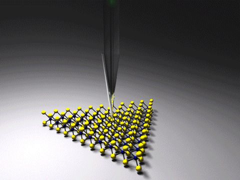
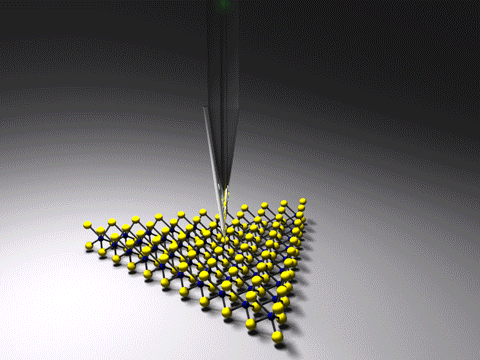
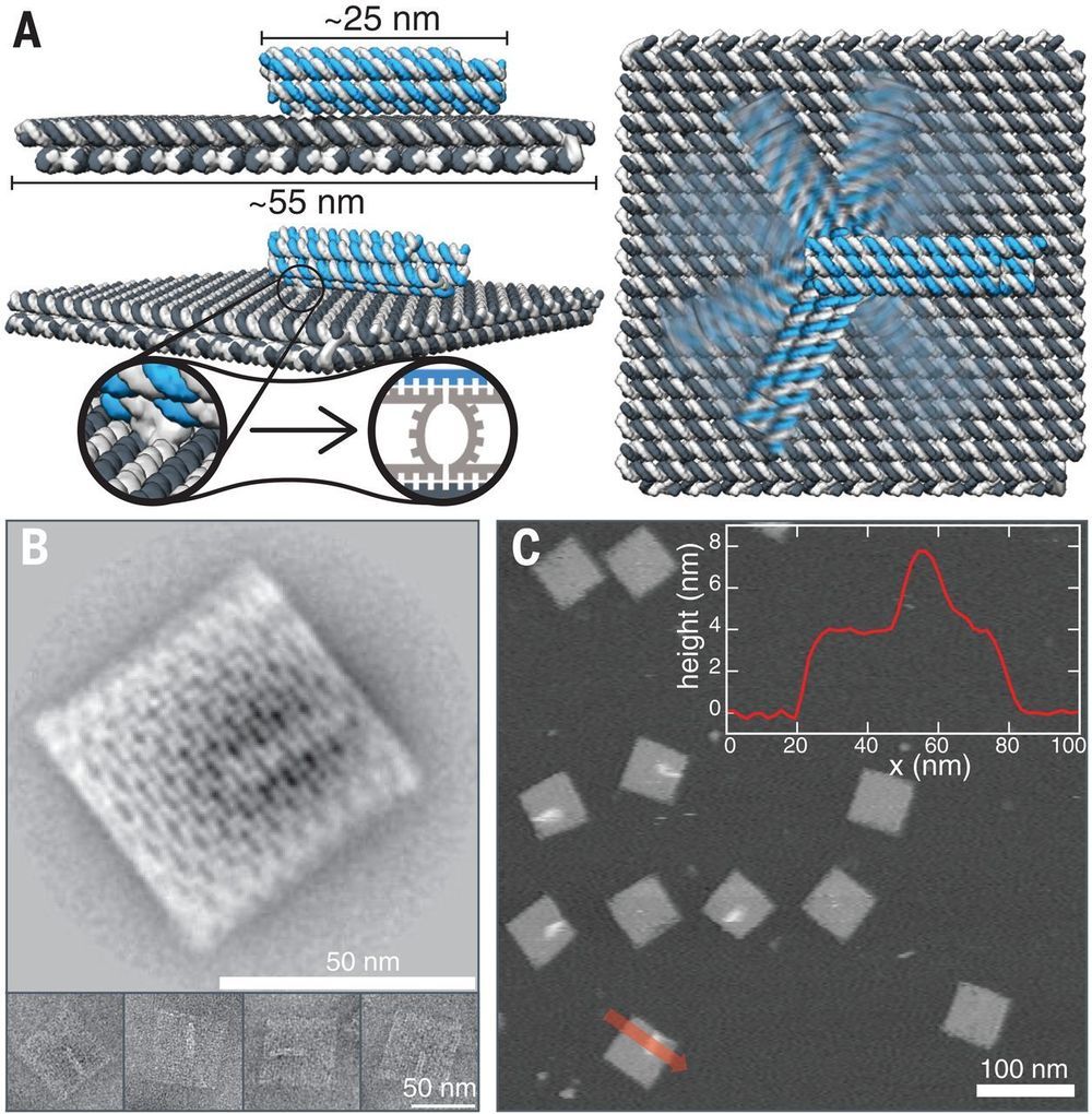
Menu

Blog

Archive for the ‘nanotechnology’ category: Page 269

Jul 7, 2016

Fantastic voyage to the nanoverse one step closer

Posted by in categories: biotech/medical, engineering, nanotechnology, particle physics, robotics/AI

Robots so small they can enter the bloodstream and perform surgeries are one step closer, a research team from Monash University has discovered.

Led by Dr Zhe Liu, the Monash Engineering team has focused on graphene oxide — which is a single atom thick — as an effective shape memory material.

Graphene has captured world scientific and industrial interest for its miracle properties, with potential applications across energy, medicine, and even biomedical nano-robots.

Continue reading “Fantastic voyage to the nanoverse one step closer” »

Jul 6, 2016

Probing Quantum Phenomena in Tiny Transistors

Posted by in categories: computing, nanotechnology, quantum physics

Nearly 1,000 times thinner than a human hair, nanowires can only be understood with quantum mechanics. Using quantum models, physicists from Michigan Technological University have figured out what drives the efficiency of a silicon-germanium (Si-Ge) core-shell nanowire transistor.

Core-Shell Nanowires

The study, published last week in Nano Letters, focuses on the quantum tunneling in a core-shell nanowire structure. Ranjit Pati, a professor of physics at Michigan Tech, led the work along with his graduate students Kamal Dhungana and Meghnath Jaishi.

Continue reading “Probing Quantum Phenomena in Tiny Transistors” »

Jul 5, 2016

Bowtie-shaped nanostructures may advance the development of quantum devices

Posted by in categories: computing, nanotechnology, particle physics, quantum physics

Bowtie-shaped nanoparticles made of silver may help bring the dream of quantum computing and quantum information processing closer to reality. These nanostructures, created at the Weizmann Institute of Science and described recently in Nature Communications, greatly simplify the experimental conditions for studying quantum phenomena and may one day be developed into crucial components of quantum devices.

The research team led by Prof. Gilad Haran of Weizmann’s Chemical Physics Department — postdoctoral fellow Dr. Kotni Santhosh, Dr. Ora Bitton of Chemical Research Support and Prof. Lev Chuntonov of the Technion-Israel Institute of Technology — manufactured two-dimensional bowtie-shaped silver nanoparticles with a minuscule gap of about 20 nanometers (billionths of a meter) in the center. The researchers then dipped the “bowties” in a solution containing quantum dots, tiny semiconductor particles that can absorb and emit light, each measuring six to eight nanometers across. In the course of the dipping, some of the quantum dots became trapped in the bowtie gaps.

Under exposure to light, the trapped dots became “coupled” with the bowties — a scientific term referring to the formation of a mixed state, in which a photon in the bowtie is shared, so to speak, with the quantum dot. The coupling was sufficiently strong to be observed even when the gaps contained a single quantum dot, as opposed to several. The bowtie nanoparticles could thus be prompted to switch from one state to another: from a state without coupling to quantum dots, before exposure to light, to the mixed state characterized by strong coupling, following such exposure.

Continue reading “Bowtie-shaped nanostructures may advance the development of quantum devices” »

Jul 4, 2016

Discovery could dramatically boost efficiency of perovskite solar cells

Posted by in categories: nanotechnology, solar power, sustainability

Scientists from the Department of Energy’s Lawrence Berkeley National Laboratory (Berkeley Lab) have discovered a possible secret to dramatically boosting the efficiency of perovskite solar cells hidden in the nanoscale peaks and valleys of the crystalline material.

Solar cells made from compounds that have the crystal structure of the mineral perovskite have captured scientists’ imaginations. They’re inexpensive and easy to fabricate, like organic solar cells. Even more intriguing, the efficiency at which perovskite solar cells convert photons to electricity has increased more rapidly than any other material to date, starting at three percent in 2009 — when researchers first began exploring the material’s photovoltaic capabilities — to 22 percent today. This is in the ballpark of the efficiency of silicon solar cells.

Now, as reported online July 4, 2016 in the journal Nature Energy, a team of scientists from the Molecular Foundry and the Joint Center for Artificial Photosynthesis, both at Berkeley Lab, found a surprising characteristic of a perovskite solar cell that could be exploited for even higher efficiencies, possibly up to 31 percent.

Read more

Jul 2, 2016

Solar nano-grids light up homes and businesses in Kenya

Posted by in categories: business, computing, economics, habitats, nanotechnology

First installations go live as INTASAVE Energy pursues $30M impact investment.

Villagers in Lemolo B and Echareria in Nakuru County, Kenya, are waking up today to a new future as new solar nano-grids installed over the last two weeks allows them to switch on lights and operate new agri-processing machinery. The two communities are the first to receive a revolutionary new model for clean, affordable and reliable energy where a central solar hub provides both commercial energy for new village enterprises and household energy using cutting-edge up-cycled laptop batteries. The hub allows energy to be shared between households, businesses and the community bringing economic, social and environmental benefits.

The installation is the start of a major INTASAVE Energy solar nano-grid initiative (SONG) that ultimately aims to bring the benefits now beginning for villagers in Lemolo B and Echareria to over 450,000 people across the globe. INTASAVE Energy has launched a $30M impact investment programme to make this goal a reality.

Continue reading “Solar nano-grids light up homes and businesses in Kenya” »

Jul 2, 2016

New material switches from water-repelling to water-loving with electric current

Posted by in categories: materials, nanotechnology

Definitely makes sense when you consider how things work in nature.


Generally, water repellent objects and those that attract or absorb water have very different microscopic-level attributes that endow them with their behavior. For example, the myriad tiny hairs on a gecko’s body help it to efficiently repel water, whilst specially treated cotton designed for harvesting water from the air contains millions of tiny pores that draw in liquid. Now researchers have discovered a way to use a single type of material to perform both functions, switching between liquid attraction and liquid repulsion, simply through the application of an electric voltage.

Developed by a team of scientists from TU Wien, the University of Zurich, and KU Levin, the new material alters its water-handling behavior by changing its surface structure at the nanoscale to effect a change at the macroscale. Specifically, the behavior of liquid on the new material is as a result of altering the “stiction” (static friction) of the molecular surface. One with a high-level of stiction keeps moisture clinging to it, whilst one with a low-level allows the liquid to run right off.

Continue reading “New material switches from water-repelling to water-loving with electric current” »

Jun 30, 2016

Rising Applications of Quantum Dots in Healthcare Industry to Drive Global Quantum Dots Market

Posted by in categories: health, nanotechnology, quantum physics, security, solar power, sustainability

Q-Dot demand in Healthcare is predicted to be high.

http://embedded-computing.com/news/rising-quantum-dots-market/#


Quantum Dots Market is driven by increasing demand for energy efficient displays and lighting solutions, North America accounted for largest quantum dots market share, use of quantum dots in solar cells and VLSI design is expected to open new possibilities for quantum dots market.

Quantum dots are semiconducting nanoparticles that range from 1nm to 10nm diameter in size and demonstrate quantum mechanical properties. The peculiarity of quantum dots is that they have ability to unite their semiconductor properties with those of nanomaterials. In addition, tunable nanocrystal size and superior optical properties have made quantum dots attractive semiconducting material for variety of applications in the field of healthcare, optoelectronics, solar energy, and security among others.

Read more

Jun 25, 2016

NASA Wants to Launch Interstellar Space Missions in 20 Years

Posted by in categories: nanotechnology, quantum physics, robotics/AI, space, time travel

The craving to explore beyond our solar system grows sturdier every day. This proves true for the understanding of wormholes and time travel as well. In order to satisfy our thirst for the unknown, NASA will research unknown physics revolutionizing exploration of space. We first have to advance our understanding of space-time, the quantum vacuum, gravity and other physical phenomena. This info will help NASA send robots on interstellar space missions. Precisely 15 areas will be studied comprising human exploration, landing systems, nanotechnology and robots.

Read more

Jun 25, 2016

Brain-like computers may now be realistic

Posted by in categories: 3D printing, biotech/medical, computing, nanotechnology, robotics/AI, transportation

Power consumption is one of the biggest reasons why you haven’t seen a brain-like computer beyond the lab: the artificial synapses you’d need tend to draw much more power than the real thing. Thankfully, realistic energy use is no longer an unattainable dream. Researchers have built nanowire synapses that consume just 1.23 femtojoules of power — for reference, a real neuron uses 10 femtojoules. They achieve that extremely low demand by using a wrap of two organic materials to release and trap ions, much like real nerve fibers.

There’s a lot of work to be done before this is practical. The scientists want to shrink their nanowires down from 200 nanometers thick to a few dozen, and they’d need new 3D printing techniques to create structures that more closely imitate real brains. Nonetheless, the concept of computers with brain-level complexity is that much more realistic — the team tells Scientific American that it could see applications in everything from smarter robots and self-driving cars through to advanced medical diagnosis.

Read more

Jun 22, 2016

Viewpoint: Hiding a Quantum Cache in Diamonds

Posted by in categories: computing, internet, nanotechnology, quantum physics

Entanglement purification, a vital enabler for practical quantum networks, has been shown to be feasible with secluded nuclear memories in diamond.

Quantum devices can team up to perform a task collectively, but only if they share that most “spooky” of all quantum phenomena: entanglement. Remote devices have been successfully entangled in order to investigate entanglement itself [1], but the entanglement’s quality is too low for practical applications. The solution, known as entanglement purification [2], has seemed daunting to implement in a real device. Now new research [3] shows that even quite simple quantum components—nanostructures in diamond—have the potential to store and upgrade entanglement. The result relies on hiding information in almost-inaccessible nuclear memories, and may be a key step toward the era of practical quantum networks.

The concept of an interlinked network is absolutely fundamental to conventional technologies. It applies not only to distributed systems like the internet, but also to individual devices like laptops, which contain a hierarchy of interlinked components. For quantum technologies to fulfill their potential, we will want them to have the flexibility and scalability that come from embracing the network paradigm.

Read more