Toggle light / dark theme

Graphene and 2-D materials could move electronics beyond ‘Moore’s law’

A team of researchers based in Manchester, the Netherlands, Singapore, Spain, Switzerland and the U.S. has published a new review on a field of computer device development known as spintronics, which could see graphene used as building block for next-generation electronics.

Recent theoretical and experimental advances and phenomena in studies of electronic spin transport in and related two-dimensional (2-D) materials have emerged as a fascinating area of research and development.

Spintronics is the combination of electronics and magnetism, at the nanoscale and could lead to next generation high-speed electronics. Spintronic devices are a viable alternative for nanoelectronics beyond Moore’s law, offering higher energy efficiency and lower dissipation as compared to conventional electronics, which relies on charge currents. In principle we could have phones and tablets operating with spin-based transistors and memories.

Researchers Propose New Diamond Nanostructure For Efficient Energy Storage

One of the biggest challenges for renewable energy research is energy storage. The goal is to find a material with high energy storage capacity and energy storage material with high storage capacity that can also quickly and efficiently discharge a large amount of energy. In an attempt to overcome this hurdle, researchers at the Queensland University of Technology (QUT) have proposed a brand-new carbon nanostructure designed to store energy in mechanical form.

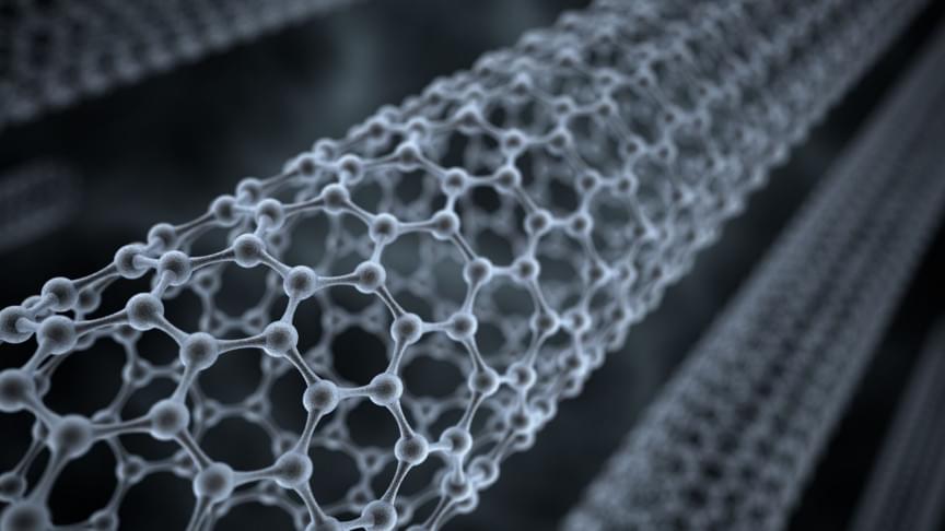
Most portable energy storage devices currently rely on storing energy in chemical form such as batteries, however this proposed new structure, made from a bundle of diamond nanothread (DNT) does not suffer from the same limiting properties as batteries, such as temperature sensitivity, or the potential to leak or explode. I have previously written about carbon nanotubes, and their applications in everything from Batman-like artificial muscle, to an analogy of the fictional element Vibranium, but a lot of research around carbon nanotubes is already focused on energy harvesting and energy storage applications.

What makes this energy storage method different is the method by which energy is stored, and also the related increased robustness of the resultant material. Dr Haifei Zhan and his team at the QUT Centre for material science used computer modelling to propose the structure of these ultra-thin one-dimensional carbon threads. The theory is that these threads should be able to store energy when they are twisted or stretched, similar to the way we store energy in wind-up toys. By turning the key, we force the spring inside into a tight coil. Once the key is released, the coil wishes to release the extra tension held within it and begins to unfurl. In doing so it transfers that mechanical energy into the movement of the toy’s wheels.

Iron Nanorobots Go Undercover to Track Living Cells Inside the Body

Customizable magnetic iron nanowires pinpoint and track the movements of target cells.

Living cells inside the body could be placed under surveillance—their location and migration noninvasively tracked in real time over many days—using a new method developed by researchers at KAUST.

The technique uses magnetic core-shell iron nanowires as nontoxic contrast agents, which can be implanted into live cells, lighting up those cells’ location inside a living organism when scanned by magnetic resonance imaging (MRI). The technique could have applications ranging from studying and treating cancer to tracking live-cell medical treatments, such as stem cell therapies.

Nanotech Breakthrough Could Revolutionize Night Vision

Circa 2016


Researchers build “teeny, tiny structures” that can change infrared to visible light.

Remember that famous Bin Laden raid? It would have been impossible without night vision — specifically, a pair of $65,000 L-3 Ground Panoramic Night Vision Goggles. But even those top-of-the-line NVGs — former Navy SEAL Matt Bissonette compared other night-vision systems to “looking through toilet paper tubes” — are heavy, clunky, and odd-looking. Now researchers from Australia have developed a material that can make infrared light visible, raising the possibility of night-vision goggles as thin as glass and free of external power.

Conventional night vision goggles look a bit like binoculars and require electricity. Here’s how they work: An “objective lens” in front collects low-level and near-infrared light, whose photons are converted by a photocathode into electrons. The goggles use thousands of volts of electricity to send the electrons down a vacuum-sealed tube into a plate with millions of tiny holes. Pushing the electrons through the holes releases other electrons in a chain reaction called cascaded secondary emission. The effect: where there was one electron, there are now hundreds, all in the same pattern as the original photons. When the electrons hit the final layer, which is covered in phosphorescent material, what was dark becomes light.

$3 Million Kavli Prizes Awarded to Scientists for Discoveries in Astrophysics, Nanoscience, Neuroscience

The Norwegian Academy of Science and Letters today announced the 2020 Kavli Prize Laureates in the fields of astrophysics, nanoscience, and neuroscience. This year’s Kavli Prize honors scientists whose research has transformed our understanding of the very big, the very small and the very complex. The laureates in each field will share USD 1 million.

This year’s Kavli Prize Laureates are:

Making Quantum ‘Waves’ in Ultrathin Materials – Plasmons Could Power a New Class of Technologies

Study co-led by Berkeley Lab reveals how wavelike plasmons could power up a new class of sensing and photochemical technologies at the nanoscale.

Wavelike, collective oscillations of electrons known as “plasmons” are very important for determining the optical and electronic properties of metals.

In atomically thin 2D materials, plasmons have an energy that is more useful for applications, including sensors and communication devices, than plasmons found in bulk metals. But determining how long plasmons live and whether their energy and other properties can be controlled at the nanoscale (billionths of a meter) has eluded many.

Teslaphoresis-activated self-assembling carbon nanotubes look even cooler than they sound

Circa 2016


Not all important scientific research is cool looking, or has a cool name. But now and then you get something with both. These self-assembling carbon nanotubes are created with a process called Teslaphoresis. If you’ve read a more impressive-sounding sentence today, I’d like to hear it.

Even the lab of Rice University chemist Paul Cherukuri looks like a proper mad scientist’s lair. But don’t let the flashy trappings fool you: this is a very significant development.

Nanotubes are one of these carbon supermaterials that, like graphene, are full of interesting properties and theoretical applications but — again like graphene — are difficult to manufacture cheaply and reliably. This new method could be a breakthrough in the creation of the ultra-thin, ultra-strong, and ultra-conductive carbon nanowires.

Anyons bunch together in a 2D conductor

Anyons – the particle-like collective excitations that can exist in some 2D materials – tend to bunch together in a two-dimensional conductor. This behaviour, which has now been observed by physicists at the Laboratory of Physics of the ENS (LPENS) and the Center for Nanoscience and Nanotechnologies (C2N) in Paris, France, is completely different to that of electrons, and experimental evidence for it is important both for fundamental physics and for the potential future development of devices based on these exotic quasiparticles.

The everyday three-dimensional world contains two types of elementary particles: fermions and bosons. Fermions, such as electrons, obey the Pauli exclusion principle, meaning that no two fermions can ever occupy the same quantum state. This tendency to flee from each other is at the heart of a wide range of phenomena, including the electronic structure of atoms, the stability of neutron stars and the difference between metals (which conduct electric current) and insulators (which don’t). Bosons such as photons, on the other hand, tend to bunch together – a gregarious behaviour that gives rise to superfluid and superconducting behaviours when many bosons exist in the same quantum state.

Within the framework of quantum mechanics, fermions also differ from bosons in that they have antisymmetric wavefunctions – meaning that a minus sign (that is, a phase φ equal to π) is introduced whenever two fermions are exchanged. Bosons, in contrast, have symmetric wavefunctions that remain the same when two bosons are exchanged (φ=0).

Electron microscopy of nanoparticle superlattice formation at a solid-liquid interface in non-polar liquids

Nanoparticle superlattice films that form at the solid-liquid interface are important for mesoscale materials but are challenging to analyze on the onset of formation at a solid-liquid interface. In a new report on Science Advances, E. Cepeda-Perez and a research team in materials, physics and chemistry in Germany studied the early stages of nanoparticle assembly at solid-liquid interfaces using liquid-phase electron microscopy. They observed oleylamine-stabilized gold nanoparticles to spontaneously form thin layers on a silicon nitride membrane window of the liquid enclosure. In the first monolayer, the assembly maintained dense packings of hexagonal symmetry independent of the nonpolar solvent type. The second layer displayed geometries ranging from dense packing in a hexagonal honeycomb structure to quasi-crystalline particle arrangements—based on the dielectric constant of the liquid. The complex structures made of weaker interactions remained preserved, while the surface remained immersed in liquid. By fine-tuning the properties of materials involved in nanoparticle superlattice formation, Cepeda-Perez et al. controlled the three-dimensional (3D) geometry of a superlattice, including quasi-crystals (a new state of matter).

Nanoparticles that are densely packed into two or three dimensions can form regular arrays of nanoparticle superlattices. For example, semiconductor particle superlattices can act as “meta” semiconductors when doped with particles to form new mesoscale materials, while plasmonic particles in dense superlattices can couple to form collective modes with angle-dependent and tunable wavelength responses. Large electric fields can occur between such particles for surface-enhanced Raman spectroscopy. Superlattices can be developed at liquid-liquid, gas-liquid and solid-liquid interfaces, where static and dynamic interactions between particle-substrate, particle-particle and particle-liquid interactions can dictate the structure of superlattices. However, it remains difficult to predict such structures in advance. For example, simulating the assembly of superlattices at multiple stages is not yet possible, with very little in-lab real-space data available for modeling.