Toggle light / dark theme

Materials formed on vanishingly small scales are being used in medicine, electronics, manufacturing and a host of other applications. But scientists have only scratched the surface of understanding how to control building blocks on the nanoscale, where simple machines the size of a virus operate.

Now, a team of researchers led by Dongsheng Li, a materials scientist at PNNL, and collaborators at the University of Michigan and the Chinese Academy of Sciences, have unlocked the secret to one of the most useful nanostructures: the five-fold twin. Their study describing why and how this shape forms is detailed in the journal Science and was presented at the Materials Research Society annual meeting on December 5, 2019.

A cross section of a five-fold twin structure looks for all the world like a pie sliced into five perfectly symmetrical pieces. Nanomaterials with this structure have already been shown to have useful properties and are deployed in for precisely tagging cancerous tumors for imaging and tracking, and in electronics, where they are valued for their mechanical strength.

Scientists at Tokyo Institute of Technology (Tokyo Tech) have developed a new methodology that allows researchers to assess the chemical composition and structure of metallic particles with a diameter of only 0.5 to 2 nm. This breakthrough in analytical techniques will enable the development and application of minuscule materials in the fields of electronics, biomedicine, chemistry, and more.

The study and development of novel materials have enabled countless technological breakthroughs and are essential across most fields of science, from medicine and bioengineering to cutting-edge electronics. The rational design and analysis of innovative materials at nanoscopic scales allows us to push through the limits of previous devices and methodologies to reach unprecedented levels of efficiency and new capabilities. Such is the case for metal nanoparticles, which are currently in the spotlight of modern research because of their myriad potential applications. A recently developed synthesis method using dendrimer molecules as a template allows researchers to create metallic nanocrystals with diameters of 0.5 to 2 nm (billionths of a meter).

On Dec. 11, 2019, a general framework for incorporating and correcting for nonclassical electromagnetic phenomena in nanoscale systems will be presented in the journal Nature.

More than 150 years have passed since the publication of James Clerk Maxwell’s “A Dynamical Theory of the Electromagnetic Field” (1865). His treatise revolutionized the fundamental understanding of electric fields, magnetic fields and light. The 20 original equations (elegantly reduced to four today), their boundary conditions at interfaces, and the bulk electronic response functions (dielectric permitivity and magnetic permeability) are at the root of the ability to manipulate electromagnetic fields and light.

Life without Maxwell’s equations would lack most current science, communications and technology.

NaNotics, in another breakthrough, is promising a new kind of medication, and suggests to have found a way to combat age related diseases; boldly going where no nanotech has gone before.

Lou Hawthorne of NaNotics, LLC opened his presentation at a recent longevity investor event using a clip from Star Trek that shows captain Kirk being giving a shot that restores him to his younger years.

“It’s tempting to assume it’s a drug, but what if the content of that syringe was something new?” NaNotics’ CEO Hawthorne asked. “NaNots are a new class of medicine. They are engineered to do just one thing and that’s the holy grail of medicine design, because most drugs do two things: something you want them to do, and something you don’t. In other words, side effects.”

I am in shock… Google suddenly as yahoo are allowing conjecture and mendacity be seen as public or scientific opinion. Here is another confused mind who towards the end of her rant quotes Christian scripture as basis to stop Life extension-Transhumanism???

When I say to these minds Behold the leader of Christianity stood for Life abundant-Super Longevity and I can prove such. No matter what lost evangelist or preacher tells you Jesus was a medical researcher of extraordinary magnitude…

NOW BEHOLD THE LOST in this article… https://www.rodofironministries.com/…/transhumanism-and-imm… Respect r.p.berry & AEWR wherein aging now ends we have found the many causes of aging and we have located an expensive cure. We search for partners-investors to now join us in agings end… gerevivify.blogspot.com/


Whether we like it or not, the hybrid age is already here. From genetic manipulation, to AI technology, to nano-technology, robotics, 3D printing, brain mapping, super computing, the list is literally endless. Futurists and Transhumanist philosophers believe that science and technology are limitless, and that humanity’s current cultural traditions and mindset are the mechanisms in place that prohibit human development.

Scientists from Tokyo Metropolitan University have used aligned “metallic” carbon nanotubes to create a device which converts heat to electrical energy (a thermoelectric device) with a higher power output than pure semiconducting carbon nanotubes (CNTs) in random networks. The new device bypasses the troublesome trade-off in semiconductors between conductivity and electrical voltage, significantly outperforming its counterpart. High power thermoelectric devices may pave the way for more efficient use of waste heat, like wearable electronics.

Thermoelectric devices can directly convert heat to electricity. When we think about the amount of wasted heat in our environment like in air conditioning exhausts, vehicle engines or even body heat, it would be revolutionary if we could somehow scavenge this energy back from our surroundings and put it to good use. This goes some way to powering the thought behind wearable electronics and photonics, devices which could be worn on the skin and powered by body heat. Limited applications are already available in the form of body heat powered lights and smartwatches.

The power extracted from a thermoelectric device when a is formed is affected by the conductivity of the device and the Seebeck coefficient, a number indicating how much electrical voltage is generated with a certain difference in temperature. The problem is that there is a trade-off between the Seebeck coefficient and conductivity: the Seebeck coefficient drops when the device is made more conductive. To generate more power, we ideally want to improve both.

A team at Samsung Advanced Institute of Technology has announced that they have improved quantum dot (QD) technology for use in large displays by developing QDs that are both more efficient and have no heavy metals. In their paper published in the journal Nature, the group describes their work and their plans for the future. Alexander Efros, with the Naval Research Laboratory, in Washington D.C. has published a companion piece in the same journal issue outlining the work by the team at Samsung.

Quantum dots are nanoscale semiconducting crystals that have unique optical and electronic properties due to quirks of quantum mechanics. Since their development in the 1980s, scientists have been finding many uses for them in optical devices. Unfortunately, as Efros notes, they suffer from two problems that have prevented them from being fully utilized. The first is that they are based on cadmium, a toxic heavy metal. The second is the QD phosphors that are used in display devices—they are not self- emissive, which means they need to be replaced by QD light-emitting diodes in order for them to be competitively efficient. Notably current Samsung QLED TV screens do not use the QLEDs as a source of light—instead, LCDs produce backlight which is then absorbed by a film of quantum dots. In this new effort, the group at Samsung has made progress towards addressing both problems.

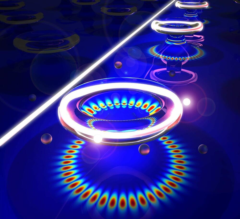
The first ever integrated nanoscale device which can be programmed with either photons or electrons has been developed by scientists in Harish Bhaskaran’s Advanced Nanoscale Engineering research group at the University of Oxford.

In collaboration with researchers at the universities of Münster and Exeter, scientists have created a first-of-a-kind electro– which bridges the fields of optical and electronic computing. This provides an elegant solution to achieving faster and more energy efficient memories and processors.

Computing at the has been an enticing but elusive prospect, but with this development it’s now in tangible proximity. Using light to encode as well as transfer information enables these processes to occur at the ultimate speed limit—that of light. While as of recently, using light for certain processes has been experimentally demonstrated, a compact device to interface with the electronic architecture of traditional computers has been lacking. The incompatibility of electrical and light-based computing fundamentally stems from the different interaction volumes that electrons and photons operate in. Electrical chips need to be small to operate efficiently, whereas need to be large, as the wavelength of light is larger than that of electrons.

Alcor calls them “patients”, and right now, over 150 of these frozen souls are waiting for the future in vats of liquid nitrogen stored in Scottsdale, Arizona. We interview Dr. Ralph Merkle, a director at the Alcor Foundation and a respected pioneer in nanotechnology, to learn how recent advances in cryonics just may enable long-haul interstellar spaceflight sooner than you’d guess…