👉For business inquiries: [email protected].
✅ Instagram: https://www.instagram.com/pro_robots.
You’re on the PRO Robots channel, and today we’re bringing you some high-tech news. Robots from Boston Dynamics will get advanced artificial intelligence, neural networks will be able to translate the language of all animals, incredibly fast nanorobots will travel inside the human body, a robot-surgeon will perform an operation on the ISS. See these and other technology news in one video right now!
0:00 Intro.
0:28 Robots from Boston Dynamics get advanced artificial intelligence.
1:52 AI will never be intelligent.
2:50 Earth Species Project hopes to develop a neural network that can decipher animal language.
3:16 Species Project decides to go around and create an algorithm.
4:07 A gadget to control your smart home with your mind.
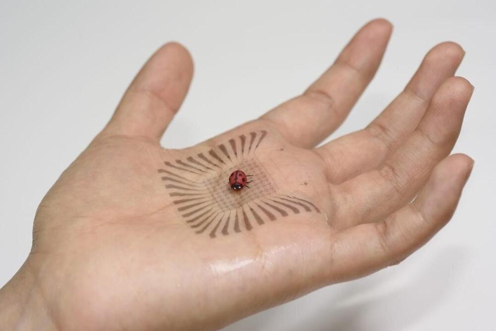
5:04 Nanobots.
5:19 The world’s fastest bowel robot.
6:10 Robots will join the U.S. space forces.
6:47 Surgical robot to be tested on ISS
7:37 GITAI News.
7:59 The first launch in NASA’s Artemis lunar mission.
8:34 Super Heavy rocket successfully passes first static firing test.
8:57 Gigafactory in Canada.
9:22 Baidu says its Jidu robot car autopilot will be a generation ahead of Tesla’s autopilot.
10:02 A system that can calculate the optimal end design and calculate the best trajectory for grabbing objects of any shape.
10:25 A drone to search for gold and jewelry.
11:22 Engineers have trained a drone with 12 rotary screws to manipulate objects.
#prorobots #robots #robot #futuretechnologies #robotics.
More interesting and useful content:
✅ Elon Musk Innovation https://www.youtube.com/playlist?list=PLcyYMmVvkTuQ-8LO6CwGWbSCpWI2jJqCQ
✅Future Technologies Reviews https://www.youtube.com/playlist?list=PLcyYMmVvkTuTgL98RdT8-z-9a2CGeoBQF
✅ Technology news.
https://www.facebook.com/PRO.Robots.Info.
#prorobots #technology #roboticsnews.
PRO Robots is not just a channel about robots and future technologies, we are interested in science, technology, new technologies and robotics in all its manifestations, science news, technology news today, science and technology news 2022, so that in the future it will be possible to expand future release topics. Today, our vlog just talks about complex things, follows the tech news, makes reviews of exhibitions, conferences and events, where the main characters are best robots in the world! Subscribe to the channel, like the video and join us!