When most people think of crystals, they picture suncatchers that act as rainbow prisms or the semi-transparent stones that some believe hold healing powers. However, to scientists and engineers, crystals are a form of materials in which their constituents—atoms, molecules, or nanoparticles—are arranged regularly in space. In other words, crystals are defined by the regular arrangement of their constituents. Common examples are diamonds, table salt, or sugar cubes.
However, in research just published in Soft Matter, a team led by Rensselaer Polytechnic Institute’s Sangwoo Lee, associate professor in the Department of Chemical and Biological Engineering, discovered that crystal structures are not necessarily always regularly arranged. The discovery advances the field of materials science and has unrealized implications for the materials used for semiconductors, solar panels, and electric vehicle technologies.
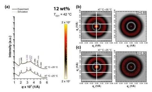
One of the most common and important classes of crystal structures is the close-packed structures of regular spheres constructed by stacking layers of spheres in a honeycomb arrangement. There are many ways to stack the layers to construct close-packed structures, and how nature selects specific stacking is an important question in materials and physics research. In the close-packing construction, there is a very unusual structure with irregularly spaced constituents known as the random stacking of two-dimensional hexagonal layers (RHCP). This structure was first observed from cobalt metal in 1942, but it has been regarded as a transitional and energetically unpreferred state.

