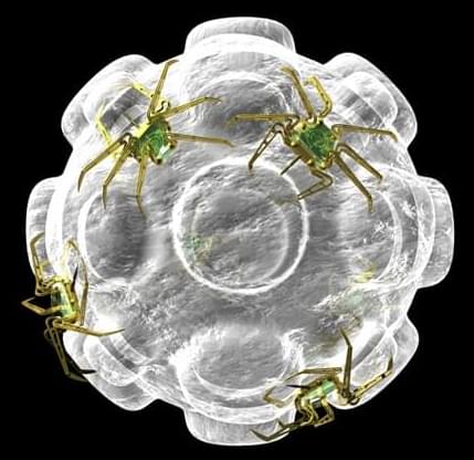
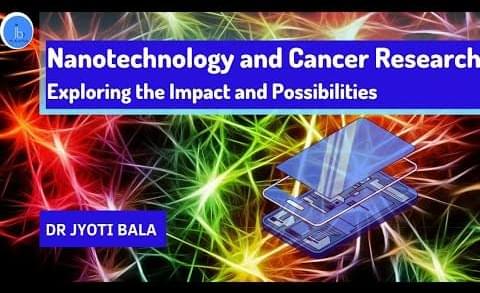
Canon is moving ahead with a plan to build a new factory in Japan to double the production of its semiconductor lithography equipment.
The planned facility will produce both the standard KrF and i-line machines that constitute the bulk of the division’s sales and the nanoimprint tools that Canon hopes will open a new era in semiconductor manufacturing.
Addressing investors after the announcement of third-quarter results in late October, Canon’s management referred to “our leading-edge nanoimprint lithography equipment.”
“IMAGINE printing out a paper computer and tearing off a corner so someone else can use part of it.” So says Steve Hodges of Microsoft Research in Cambridge, UK. The idea sounds fantastical, but it could become an everyday event thanks in part to a technique he helped develop.
Hodges, along with Yoshihiro Kawahara and his team at the University of Tokyo, Japan, have found a way to print the fine, silvery lines of electronic circuit boards onto paper. What’s more, they can do it using ordinary inkjet printers, loaded with ink containing silver nanoparticles. Last month Kawahara demonstrated a paper-based moisture sensor at the Ubicomp conference in Zurich, Switzerland.
Kawahara says the idea is perfect for the growing maker movement of inventors and tinkerers. Hobbyists will be able to test circuit designs by simply printing them out and throwing away anything that doesn’t work. That will reduce much of electronics to a craft akin to “sewing or origami”, he says.
A new nanoscale 3D printing material developed by Stanford University engineers may provide superior structural protection for satellites, drones, and microelectronicsAn improved lightweight, a protective lattice that can absorb twice as much energy as previous materials of a similar density has been developed by engineers for nanoscale 3D printing.
According to the study led by Stanford University, a nanoscale 3D printing material, which creates structures that are a fraction of the width of a human hair, will enable to print of materials that are available for use, especially when printing at very small scales.
Phuchit/iStock.
An improved lightweight, a protective lattice that can absorb twice as much energy as previous materials of a similar density has been developed by engineers for nanoscale 3D printing.
Scientists from the Department of Mechanical Engineering at Osaka University introduced a method for manufacturing complex microrobots driven by chemical energy using in situ integration. By 3D-printing and assembling the mechanical structures and actuators of microrobots inside a microfluidic chip, the resulting microrobots were able to perform desired functions, like moving or grasping. This work may help realize the vision of microsurgery performed by autonomous robots.
As medical technology advances, increasingly complicated surgeries that were once considered impossible have become reality. However, we are still far away from a promised future in which microrobots coursing through a patient’s body can perform procedures, such as microsurgery or cancer cell elimination.
Although nanotech methods have already mastered the art of producing tiny structures, it remains a challenge to manipulate and assemble these constituent parts into functional complex robots, especially when trying to produce them at a mass scale. As a result, the assembly, integration and reconfiguration of tiny mechanical components, and especially movable actuators driven by chemical energy, remains a difficult and time-consuming process.
Oregon State University scientists have invented a way to make magnetic nanoparticles that get hotter than any previous nanoparticle, improving their cancer fighting ability.
Faculty from the OSU College of Pharmacy spearheaded a collaboration that developed an advanced thermal decomposition method for producing nanoparticles able to reach temperatures in cancer lesions of up to 50 degrees Celsius, or 122 degrees Fahrenheit, when exposed to an alternating magnetic field.
Findings of the preclinical study led by Oleh Taratula and Olena Taratula were published today in the journal Small Methods.
Visit our sponsor, Brilliant: https://brilliant.org/IsaacArthur/ Every day brings us new technological advances, today we’ll explore many of those of such as robotics, automation, rapid delivery, education, medical science, nanotechnology, and more.
To design better rechargeable ion batteries, engineers and chemists from the University of Illinois Urbana-Champaign collaborated to combine a powerful new electron microscopy technique and data mining to visually pinpoint areas of chemical and physical alteration within ion batteries.
A study led by materials science and engineering professors Qian Chen and Jian-Min Zuo is the first to map out altered domains inside rechargeable ion batteries at the nanoscale—a 10-fold or more increase in resolution over current X-ray and optical methods.
The findings are published in the journal Nature Materials.
First insights into engineering crystal growth by atomically precise metal nanoclusters have been achieved in a study performed by researchers in Singapore, Saudi Arabia and Finland. The work was published in Nature Chemistry.
Ordinary solid matter consists of atoms organized in a crystal lattice. The chemical character of the atoms and lattice symmetry define the properties of the matter, for instance, whether it is a metal, a semiconductor or and electric insulator. The lattice symmetry may be changed by ambient conditions such as temperature or high pressure, which can induce structural transitions and transform even an electric insulator to an electric conductor, that is, a metal.
Larger identical entities such as nanoparticles or atomically precise metal nanoclusters can also organize into a crystal lattice, to form so called meta-materials. However, information on how to engineer the growth of such materials from their building blocks has been scarce since the crystal growth is a typical self-assembling process.