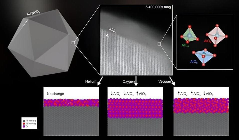
Toggle light / dark theme

Researchers solve temperature problem for source-gated transistors

Low-cost, flexible displays that use very little energy could be a step closer, thanks to an innovation from the University of Surrey that solves a problem that has plagued source-gated transistors (SGT). The study has been published by IEEE Transactions on Electron Devices.

Dr. Radu Sporea, project lead from the University of Surrey, said, We used a rapidly emerging semiconductor material called IGZO or indium-gallium-zinc oxide to create the next generation of source-gated transistors. Through nanoscale contact engineering, we obtained transistors that are much more stable with temperature than previous attempts. Device simulations allowed us to understand this effect.

This new design adds to SGTs and retains usual benefits like using low power, producing high signal amplification, and being more reliable under different conditions. While source-gated transistors are not mainstream because of a handful of performance limitations, we are steadily chipping away at their shortcomings.

Extreme DNA resolution: Spatially multiplexed single-molecule translocations through a nanopore at controlled speeds

Aleksandra Radenovic, head of the Laboratory of Nanoscale Biology in the School of Engineering, has worked for years to improve nanopore technology, which involves passing a molecule like DNA through a tiny pore in a membrane to measure an ionic current. Scientists can determine DNA’s sequence of nucleotides—which encodes genetic information—by analyzing how each one perturbs this current as it passes through. The research has been published in Nature Nanotechnology.

Currently, the passage of molecules through a and the timing of their analysis are influenced by random physical forces, and the rapid movement of molecules makes achieving high analytical accuracy challenging. Radenovic has previously addressed these issues with optical tweezers and viscous liquids. Now, a collaboration with Georg Fantner and his team in the Laboratory for Bio-and Nano-Instrumentation at EPFL has yielded the advancement she’s been looking for—with results that could go far beyond DNA.

“We have combined the sensitivity of nanopores with the precision of scanning ion conductance microscopy (SICM), allowing us to lock onto specific molecules and locations and control how fast they move. This exquisite control could help fill a big gap in the field,” Radenovic says. The researchers achieved this control using a repurposed state-of-the-art scanning ion conductance microscope, recently developed at the Lab for Bio-and Nano-Instrumentation.

KISS: A New Way To Easily Produce Large, Clean 2D Materials

Nearly two decades have passed since the advent of graphene.

Graphene is an allotrope of carbon in the form of a single layer of atoms in a two-dimensional hexagonal lattice in which one atom forms each vertex. It is the basic structural element of other allotropes of carbon, including graphite, charcoal, carbon nanotubes, and fullerenes. In proportion to its thickness, it is about 100 times stronger than the strongest steel.

Researchers invent low-temperature synthesis method for high-quality tellurium nanomesh for next-generation electronics

A collaborative team led by researchers from City University of Hong Kong (CityU) recently invented an innovative method for synthesizing high-quality, semiconducting nanomesh at a lower temperature and production cost than conventional methods. The findings will help enable the large-scale production of nanomesh for next-generation electronics.

Nanomesh is a nano-scale material formed from a network of nanowires. For several decades, one-dimensional materials like nanowires made of crystalline inorganic materials have been widely explored as the main driver for emerging electronics, as they have features like mechanical flexibility, energy efficiency and optical transparency. However, the scalability, integrability and cost-effectiveness of nanowire semiconductors are insufficient, limiting their potential for large-area electronic and optoelectronic applications.

To overcome these shortcomings, a research team led by CityU scientists made a breakthrough, inventing a low-temperature vapor-phase growth method, which can achieve large-scale synthesis of semiconducting tellurium (Te) nanomesh for use in devices.

Triplex Origami: A Game-Changer in Gene Therapy and DNA Nanotechnology

Researchers from the Gothelf lab at Aarhus University.

Established in Aarhus, Denmark in 1928, Aarhus University (AU) is the largest and second oldest research university in Denmark. It comprises four faculties in Arts, Science and Technology, Health, and Business and Social Sciences and has a total of 27 departments. (Danish: Aarhus Universitet.)

Tiny nanopores can contribute to faster identification of diseases

In a collaboration with Groningen University, Professor Jørgen Kjems and his research group at Aarhus University have achieved a remarkable breakthrough in developing tiny nano-sized pores that can contribute to better possibilities for, among other things, detecting diseases at an earlier stage.

Their work, recently published in the journal ACS Nano, shows a new innovative method for finding specific proteins in complex biological fluids, such as blood, without having to label the proteins chemically. The research is an important milestone in , and could revolutionize medical diagnostics.

Nanopores are tiny channels formed in materials, that can be used as sensors. The researchers, led by Jørgen Kjems and Giovanni Maglia (Groningen Univ.), have taken this a step further by developing a special type of called ClyA with scanner molecules, called nanobodies, attached to it.

New material transforms light, creating new possibilities for sensors

A group of scientists and engineers that includes researchers from The University of Texas at Austin have created a new class of materials that can absorb low energy light and transform it into higher energy light. The new material is composed of ultra-small silicon nanoparticles and organic molecules closely related to ones utilized in OLED TVs. This new composite efficiently moves electrons between its organic and inorganic components, with applications for more efficient solar panels, more accurate medical imaging and better night vision goggles.

The material is described in a new paper in Nature Chemistry.

“This process gives us a whole new way of designing materials,” said Sean Roberts, an associate professor of chemistry at UT Austin. “It allows us to take two extremely different substances, silicon and , and bond them strongly enough to create not just a mixture, but an entirely new hybrid material with properties that are completely distinct from each of the two components.”

Novak Djokovic wins French Open with his ‘nanotech’ patch, but what is it?

Called TaoPatch, the device has nanocrystals that use body heat to function, but does it really work?

Serbian tennis player Novak Djokovic secured his name in tennis history by winning a record 23rd Grand Slam tournament at the French Open in Paris last night, defeating the Norwegian Casper Ruud in the final.

The win takes him ahead of Spaniard Rafael Nadal (22) and Swiss legend Roger Federer (20) for the most Grand Slam wins ever n the history of the sport.

Revolution in neuroscience: 2D nanomaterials propel advances in brain repair, treatment, and diagnosis

Review discusses the increasing importance of two-dimensional nanomaterials like graphene in neuroscience, highlighting their potential in nerve repair, creating brain-mimicking synaptic devices, and treating neurological disorders. It also considers the challenges and future prospects of these materials in this complex field.