Toggle light / dark theme

Working with one of the world’s preeminent thermoelectric materials researchers, a team of researchers in the Clemson Department of Physics and Astronomy and the Clemson Nanomaterials Institute (CNI) has developed a new, fool-proof method to evaluate thermoelectric materials.

Department of Physics and Astronomy Research Assistant Professor Sriparna Bhattacharya, Engineer Herbert Behlow, and CNI Founding Director Apparao Rao collaborated with world-renowned researcher H. J. Goldsmid, professor emeritus at the University of New South Wales (UNSW) in Sydney, Australia, to create a one-stop method for evaluating the efficiency of .

Goldsmid is considered by many to be the “father of thermoelectrics” for his pioneering work in thermoelectric materials. Bhattacharya first connected with Goldsmid on LinkedIn, telling him she had confirmed one of his theoretical predictions during her graduate studies at Clemson University.

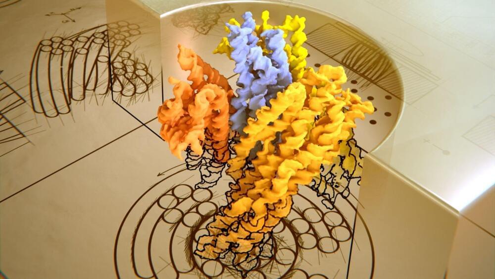
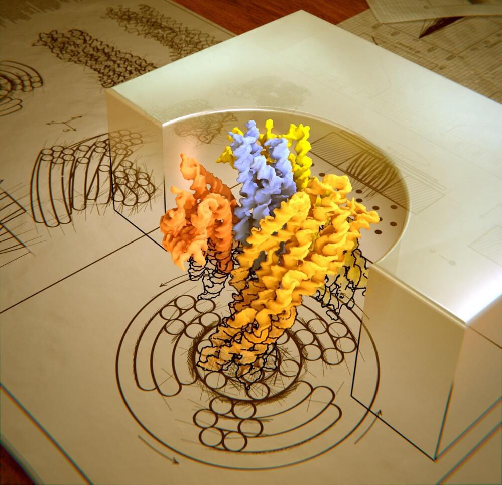
Ralph Lydic, professor in the UT Department of Psychology, and Dmitry Bolmatov, a research assistant professor in the UT Department of Physics and Astronomy, are part of a UT/ORNL research team studying how bio-inspired materials might inform the design of next-generation computers. Their results, published recently in the Proceedings of the National Academy of Sciences, could have big implications for both edge computing and human health.

Scientists at ORNL and UT discovered an artificial is capable of long-term potentiation, or LTP, a hallmark of biological learning and memory. This is the first evidence that a cell alone—without proteins or other biomolecules embedded within it—is capable of LTP that persists for many hours. It is also the first identified nanoscale structure in which memory can be encoded.

“When facilities were shut down as a result of COVID, this led us to pivot away from our usual membrane research,” said John Katsaras, a biophysicist in ORNL’s Neutron Sciences Directorate specializing in neutron scattering and the study of biological membranes at ORNL. “Together with postdoc Haden Scott, we decided to revisit a system previously studied by Pat Collier and co-workers, this time with an entirely different electrical stimulation protocol that we termed ‘training.’”.

A new miniscule nitrogen dioxide sensor could help protect the environment from vehicle pollutants that cause lung disease and acid rain.

Researchers from TMOS, the Australian Research Council Center of Excellence for Transformative Meta-Optical Systems have developed a sensor made from an array of nanowires, in a square one fifth of a millimeter per side, which means it could be easily incorporated into a silicon chip.

In research published in the latest issue of Advanced Materials, Ph.D. scholar at the Center’s Australian National University team and lead author Shiyu Wei describes the sensor as requiring no , as it runs on its own solar powered generator.

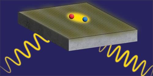
The way electrons interact with photons of light is a vital part of many modern technologies, from lasers to solar panels to LEDs. But the interaction is inherently weak because of a major mismatch in scale: the wavelength of visible light is about 1,000 times larger than an electron, so the way the two things affect each other is limited by that disparity.

Now, researchers at The University of Hong Kong (HKU), MIT and other universities say they have come up with an innovative way to make more robust interactions between photons and electrons possible, that produces a hundredfold increase in the emission of light from a phenomenon called Smith-Purcell radiation. The findings have potential ramifications for both and fundamental scientific research, although it will require more years of investigation to put into practice.

The findings are published in Nature by Dr. Yi Yang (Assistant Professor of the Department of Physics at HKU and a former postdoc at MIT), Dr. Charles Roques-carmes (Postdoctoral Associate at MIT) and Professors Marin Soljačić and John Joannopoulos (MIT professors). The research team also included Steven Kooi at MIT’s Institute for Soldier Nanotechnologies, Haoning Tang and Eric Mazur at Harvard University, Justin Beroz at MIT, and Ido Kaminer at Technion-Israel Institute of Technology.

Researchers from Carnegie Mellon University and the Chinese University of Hong Kong have developed a strategy for creating ultrahigh-resolution, complex 3D nanostructures out of various materials.

Carnegie Mellon University’s Yongxin (Leon) Zhao and the Chinese University of Hong Kong’s Shih-Chi Chen have a big idea for manufacturing nanodevices.

Zhao’s Biophotonics Lab develops novel techniques to study biological and pathological processes in cells and tissues. Through a process called , the lab works to advance techniques to proportionally enlarge microscopic samples embedded in a hydrogel, allowing researchers to be able to view fine details without upgrading their microscopes.

Chemists from Rice University and the University of Texas at Austin discovered more isn’t always better when it comes to packing charge-acceptor molecules on the surface of semiconducting nanocrystals.

The combination of organic and inorganic components in hybrid nanomaterials can be tailored to capture, detect, convert or control light in unique ways. Interest in these materials is high, and the pace of scientific publication about them has grown more than tenfold over the past 20 years. For example, they could potentially improve the efficiency of solar power systems by harvesting energy from wavelengths of sunlight—like infrared—that are missed by traditional photovoltaic solar panels.

To create the materials, chemists marry nanocrystals of light-capturing semiconductors with “charge acceptor” molecules that act as , attaching to the semiconductor’s surface and transporting electrons away from the nanocrystals.

The Seebeck effect is a thermoelectric phenomenon by which a voltage or current is generated when a temperature difference exists across a conductor. This effect is the basis of established and emerging thermoelectric applications alike, such as heat-to-electricity energy harvesters, sensing devices, and temperature control.

In line with the unrelenting demand for ever-smaller devices, scientists are looking for new ways to leverage the Seebeck effect at the nanoscale. One way to achieve this is by using molecular junctions, which are miniature devices consisting of two electrodes bridged by one or a few individual molecules. Depending on how sensitive these molecules are to temperature, it is possible to fine tune the thermoelectric properties of molecular junctions to match their intended application.

Thus far, most studies on molecular thermoelectrics have been limited to rather simple organic molecules. This has led to molecular junctions with a low Seebeck coefficient, which translates to poor temperature-to-voltage conversion and performance. There is therefore an ongoing challenge to design molecular junctions with better characteristics and, most importantly, a higher Seebeck coefficient.