Archive for the ‘materials’ category: Page 258
Sep 14, 2016
In Search of the Next Circuit Building Method – ORNL has Ideas
Posted by Karen Hurst in category: materials
Awesome @ my friends at ORNL! Luv it and expect much success too.
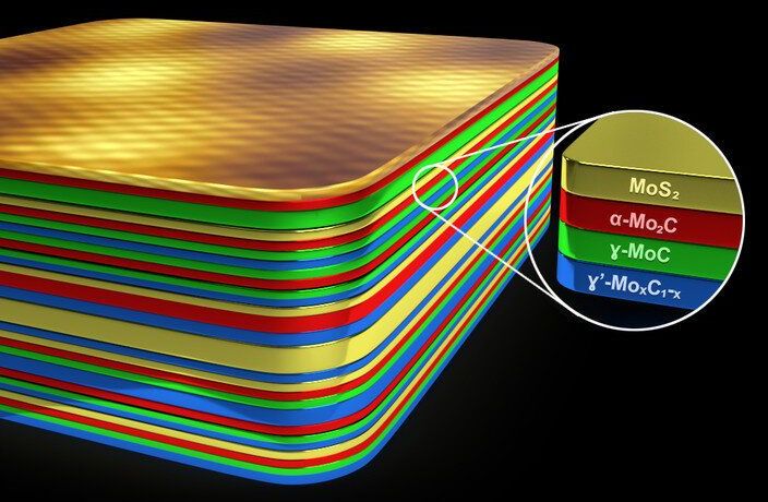
No one knows what the next, best way to build electronic circuits will be. That said there’s no shortage of efforts to invent something beyond current lithography. Oak Ridge National Laboratory, perhaps not surprisingly, is in the thick of the race and two recent studies from ORNL researchers showcase promising but very different approaches.
One method suggests phase change in a single complex oxide material may allow “creating” circuit elements much smaller than in today’s CMOS process while a second study puts STEM (scanning transmission electron microscopy) to work directly writing tiny patterns in metallic “ink,” forming features in liquid that are finer than half the width of a human hair. Articles describing both are posted on the ORNL web site.
Continue reading “In Search of the Next Circuit Building Method – ORNL has Ideas” »
Sep 12, 2016
One-pot synthesis towards sulfur-based organic semiconductors
Posted by Karen Hurst in category: materials
Advancing efforts around Synthetic Bio into the semiconductor space.
“We hope that ongoing advances in our method may lead to the development of new organic electronic devices, including semiconductor and luminescent materials,” say Segawa and Itam.
Thiophene-fused polycyclic aromatic hydrocarbons (PAHs) are known to be useful as organic semiconductors due to their high charge transport properties. Scientists have developed a short route to form various thiophene-fused PAHs by simply heating mono-functionalized PAHs with sulfur. This new method is expected to contribute towards the efficient development of novel thiophene-based electronic materials.
Exclusive: When Israel launched a covert scheme to steal material and secrets to build a nuclear bomb, U.S. officials looked the other way and obstructed investigations, as described in a book reviewed by James DiEugenio.
By James DiEugenio
In 1968, CIA Director Richard Helms was presented with a disturbing National Intelligence Estimate (NIE) stating that Israel had obtained atomic weapons, a dangerous development that occurred earlier than the CIA had anticipated.
Sep 8, 2016
Sound-proof metamaterial inspired by spider webs
Posted by Karen Hurst in category: materials
Spider silk is well-known for its unusual combination of being both lightweight and extremely strong—in some cases, stronger than steel. Due to these properties, researchers have been developing spider-silk-inspired materials for potential applications such as durable yet lightweight clothing, bullet-proof vests, and parachutes.
But so far, the acoustic properties of spider webs have not yet been explored. Now in a new study, a team of researchers from Italy, France and the UK has designed an acoustic metamaterial (which is a material made of periodically repeating structures) influenced by the intricate spider web architecture of the golden silk orb-weaver, also called the Nephila spider.
“There has been much work in the field of metamaterials in recent years to find the most efficient configurations for wave attenuation and manipulation,” coauthor Federico Bosia, a physicist at the University of Torino in Italy, told Phys.org. “We have found that the spider web architecture, combined with the variable elastic properties of radial and circumferential silk, is capable of attenuating and absorbing vibrations in wide frequency ranges, despite being lightweight.”
Continue reading “Sound-proof metamaterial inspired by spider webs” »
Sep 1, 2016
Oak Ridge Just Entered Record Books With The Largest 3D-Printed Object in the World
Posted by Karen Hurst in categories: 3D printing, materials
My friends at ORN setting records again.
Researchers at the Oak Ridge National Laboratory broke a world record for the largest solid 3D-printed item with its trim-and-drill tool. The item, which is practically the size of a large SUV, took 30 hours to print using carbon fiber and composite plastic materials.
Sep 1, 2016
Repairing Hearts With Hydrogel
Posted by Elmar Arunov in categories: biotech/medical, materials
Aug 31, 2016
DARPA Researchers Develop Novel Method for Room-Temperature Atomic Layer Deposition
Posted by Karen Hurst in category: materials
Nice.
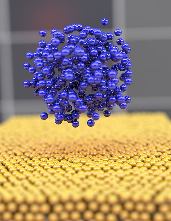
DARPA-supported researchers have developed a new approach for synthesizing ultrathin materials at room temperature—a breakthrough over industrial approaches that have demanded temperatures of 800 degrees Celsius or more. The advance opens a path to creating a host of previously unattainable thin-film microelectronics, whose production by conventional methods has been impossible because many components lose their critical functions when subjected to high temperatures.
The new method, known as electron-enhanced atomic layer deposition (EE-ALD), was recently developed at the University of Colorado, Boulder (CU) as part of DARPA’s Local Control of Materials Synthesis (LoCo) program. The CU team demonstrated room-temperature deposition of silicon and gallium nitride—linchpin elements in many advanced microelectronics—as well as the ability to controllably etch specific materials, leading to precise spatial control in three dimensions. Such a capability is critical as the demand grows for ever-smaller device architectures.
After first demonstrating the process in early 2015, team members went on to perform detailed mechanistic studies to learn how best to exploit and control EE-ALD for film growth. By controlling the electron energy during the ALD cycles, they discovered that they could tune the process to favor either material deposition or removal. The ability to selectively remove (etch) deposited material with electrons under conditions as low as room temperature is unprecedented and is anticipated to enhance film quality. The group is also exploring other methods to etch specific materials—such as aluminum nitride and hafnium oxide, important in specialized electronics applications—showing that they can selectively etch these materials in composites, which provides an attractive alternative to traditional masking approaches.
Aug 27, 2016
Going beyond 3D printing to add a new dimension for additive manufacturing
Posted by Karen Hurst in categories: 3D printing, materials
A team of Lawrence Livermore National Laboratory researchers has demonstrated the 3D printing of shape-shifting structures that can fold or unfold to reshape themselves when exposed to heat or electricity. The micro-architected structures were fabricated from a conductive, environmentally responsive polymer ink developed at the Lab.
In an article published recently by the journal Scientific Reports (link is external), Lab scientists and engineers revealed a strategy for creating boxes, spirals and spheres from shape memory polymers (SMPs), bio-based “smart” materials that exhibit shape-changes when resistively heated or when exposed to the appropriate temperature.
Continue reading “Going beyond 3D printing to add a new dimension for additive manufacturing” »
Aug 26, 2016
Construction Corner: Growing materials on demand where they’re needed
Posted by Karen Hurst in category: materials
Nice read on DARPA’s Engineered Living Materials (ELM) program. DARPA’s program to improve the quality of cell circuitry and other synthetic bios.