Menu

Blog

Archive for the ‘materials’ category: Page 170

Jan 6, 2021

This boat could help remove plastic trash from the world’s rivers

Posted by in category: materials

This video shows a boat developed to remove plastic waste from rivers.

Jan 6, 2021

Study demonstrates the quenching of an antiferromagnet into high resistivity states

Posted by in categories: materials, particle physics

Antiferromagnetism is a type of magnetism in which parallel but opposing spins occur spontaneously within a material. Antiferromagnets, materials that exhibit antiferromagnetism, have advantageous characteristics that make them particularly promising for fabricating spintronic devices.

In contrast with conventional electronic devices, which use the electrical charge of electrons to encode information, spintronics process information leveraging the intrinsic angular momentum of electrons, a property known as “spin.” Due to their ultrafast nature, their insensitivity to and their lack of magnetic stray fields, antiferromagnets could be particularly desirable for the development of spintronic devices.

Despite their advantages and their ability to store information, most simple antiferromagnets have weak readout magnetoresistivity signals. Moreover, so far physicists have been unable to change the magnetic order of antiferromagnets using optical techniques, which could ultimately allow device engineers to exploit these materials’ ultrafast nature.

Jan 6, 2021

Groundbreaking Experiment Tracks the Real-Time Transport of Individual Molecules

Posted by in categories: materials, particle physics

Oak Ridge National Laboratory’s Center for Nanophase Materials Sciences, or CNMS, contributed to a groundbreaking experiment published in Science that tracks the real-time transport of individual molecules.

A team led by the University of Graz, Austria, used unique four-probe scanning tunneling microscopy, or STM, to move a single molecule between two independent probes and observe it disappear from one point and instantaneously reappear at the other.

The STM, made available via the CNMS user program, operates under an applied voltage, scanning material surfaces with a sharp probe that can move atoms and molecules by nudging them a few nanometers at a time. This instrument made it possible to send and receive dibromoterfluorene molecules 150 nanometers across a silver surface with unprecedented control.

Jan 3, 2021

Burundi: Farmer finds new technique for preserving tomatoes

Posted by in category: materials

“He uses ash from a chimney, and sifts it three or four times to remove large residues, debris, and other foreign materials. Then, he dumps the ash into a paper carton and places the tomatoes in the carton. With this technique, Mr. Nduwimana manages to safely store his tomatoes for many months. He explains: “I keep my tomatoes in the ash for a period of five to six months, so I can sell them in December, January, or February when the price has risen—since tomatoes are rare and become expensive during this period.””


Vital Nduwimana hated how many tomatoes he lost every season. For years, his tomatoes started rotting just three or four days after harvest. He felt frustrated.

Mr. Nduwimana explains: “I was not able to sell all my tomatoes; I lost almost half of my production. Worse still, I would sell at a low price in the market. So in 2015, I thought that maybe I should find a tomato conservation technique.”

Continue reading “Burundi: Farmer finds new technique for preserving tomatoes” »

Jan 3, 2021

Inside Singapore’s huge bet on vertical farming

Posted by in categories: food, materials

From the outside, VertiVegies looked like a handful of grubby shipping containers put side by side and drilled together. A couple of meters in height, they were propped up on a patch of concrete in one of Singapore’s nondescript suburbs. But once he was inside, Ankesh Shahra saw potential. Huge potential.

Shahra, who wears his dark hair floppy and his expensive-looking shirts with their top button casually undone, had a lot of experience in the food industry. His grandfather had founded the Ruchi Group, a corporate powerhouse in India with offshoots in steel, real estate, and agriculture; his father had started Ruchi Soya, a $3 billion oilseed processor that had been Shahra’s training ground.

Jan 2, 2021

Extremely energy efficient microprocessor developed using superconductors

Posted by in categories: computing, materials

Researchers from Yokohama National University in Japan have developed a prototype microprocessor using superconductor devices that are about 80 times more energy efficient than the state-of-the-art semiconductor devices found in the microprocessors of today’s high-performance computing systems.

As today’s technologies become more and more integrated in our daily lives, the need for more is ever increasing. Because of this increase, the of that increasing computational power is growing immensely. For example, so much energy is used by modern day data centers that some are built near rivers so that the flowing water can be used to cool the machinery.

“The digital communications infrastructure that supports the Information Age that we live in today currently uses approximately 10% of the global electricity. Studies suggest that in the , if there is no fundamental change in the underlying technology of our communications infrastructure such as the computing hardware in large data centers or the electronics that drive the communication networks, we may see its electricity usage rise to over 50% of the global electricity by 2030,” says Christopher Ayala, an associate professor at Yokohama National University, and lead author of the study.

Dec 28, 2020

New chemistry for controlling the volume of liquid in volumetric additive manufacturing

Posted by in categories: chemistry, materials

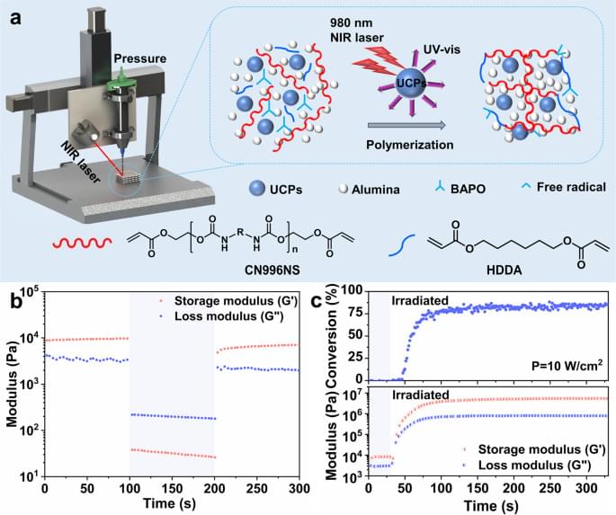
A team of researchers affiliated with several institutions in Germany has developed new chemistry for improved control of the volume of liquid in volumetric additive manufacturing. In their paper published in the journal Nature, the group describes their process and how well it worked when tested.

Three-dimensional has made many headlines over the past decade as it has revolutionized the for a wide variety of products. Most 3D printing involves controlling gantries that work together to position a nozzle that applies different types of material to a base to build products. More recently, some new types of 3D printers have been developed for volumetric additive manufacturing, or VAM, that use light to induce polymerization in a liquid to create products. They work by building products a layer at a time. In this new effort, the researchers have improved the way that polymerization starts in VAM applications. By adding the ability to control the volume of liquid precursor involved in the initiation process, they were able to increase the resolution of VAM printing by 10 times. They call their newly improved process xolography because it involves the use of two crossing light beams to solidify a desired object.

The process begins with creating a rectangular sheet of light using a laser fired into a tub of liquid precursor. The laser excites the precursor molecules inside of the rectangle, preparing them for the second beam of light. The second laser is then directed into the rectangle as a preformed image slice. When the slice is projected into the rectangle, the excited precursor molecules solidify into a polymer, forming a solidified slice. The resin volume is then moved (the sheet remains fixed in place) so that the process can be repeated to create another slice. The overall process is repeated, creating more slices as it goes, until the desired shape is achieved.

Dec 27, 2020

Two Men Created ‘Vegan Leather’ From Cactus to Save Animals and the Environment

Posted by in category: materials

Cactus leather! 😃


The quest for vegan leather is a never-ending one, as more and more researchers are focusing on finding alternative materials to real leather and create a cruelty-free world.

Continue reading “Two Men Created ‘Vegan Leather’ From Cactus to Save Animals and the Environment” »

Dec 27, 2020

We Might Have Just Found the Next Great Lighting Material

Posted by in categories: computing, materials

Researchers in Switzerland have found a new organic light emitting diode (OLED) material that could scale the technology up to inexpensively light entire rooms and homes for the first time. The results come from a new arrangement of copper electrons, CuPCP, that replaces more costly precious metal diodes (PHOLEDs). Let’s have some alphabet soup and learn about OLEDs.

Dec 27, 2020

Clean Energy Breakthrough: Scientists Improve Light-Driven Water-Splitting to Produce Hydrogen

Posted by in categories: materials, particle physics

Hydrogen is a clean energy source that can be produced by splitting water molecules with light. However, it is currently impossible to achieve this on a large scale. In a recent breakthrough, scientists at Tokyo University of Science, Japan, developed a novel method that uses plasma discharge in solution to improve the performance of the photocatalyst in the water-splitting reaction. This opens doors to exploring a number of photocatalysts that can help scale-up this reaction.

The ever-worsening global environmental crisis, coupled with the depletion of fossil fuels, has motivated scientists to look for clean energy sources. Hydrogen (H2) can serve as an eco-friendly fuel, and hydrogen generation has become a hot research topic. While no one has yet found an energy-efficient and affordable way to produce hydrogen on a large scale, progress in this field is steady and various techniques have been proposed.

One such technique involves using light and catalysts (materials that speed up reactions) to split water (H2O) into hydrogen and oxygen. The catalysts have crystalline structures and the ability to separate charges at the interfaces between some of their sides. When light hits the crystal at certain angles, the energy from the light is absorbed into the crystal, causing certain electrons to become free from their original orbits around atoms in the material. As an electron leaves its original place in the crystal, a positively charged vacancy, known as a hole, is created in the structure. Generally, these “excited” states do not last long, and free electrons and holes eventually recombine.