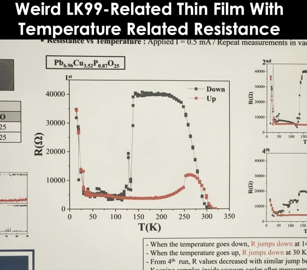
Furthermore, the experimental values are introduced to correct the adsorption isotherms. For example, Fig. 3b shows the Langmuir adsorption isotherm obtained by fitting both the predicted and experimental adsorption data. While we use simulated datasets to address data scarcity, we can also properly introduce experimental values to correct adsorption isotherms, which helps a more quantitative prediction of adsorption performance at high-pressure where the gas-gas interaction becomes more significant. In Fig. 3b, one can observe that the corrected adsorption isotherms have a strong correlation with experimental adsorption capacity to some extent. The results exhibit that Uni-MOF not only has the ability to screen the adsorption performance of the same gas in different materials but also can accurately screen the adsorption performance of different gases in the same material (Fig. 3c, d) or at different temperatures (Fig. 3e, f).
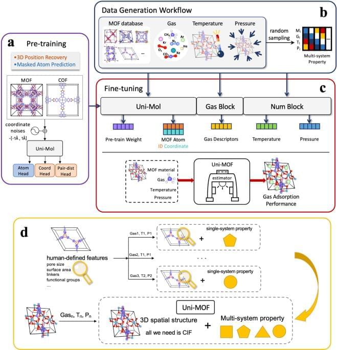
In the foreseeable future, the intersection of Artificial Intelligence (AI) and materials science will necessitate the resolution of practical and scientific issues. Nonetheless, the attainment of process implementation by AI in the realm of machine learning techniques that entail copious amounts of data remains a formidable challenge, given the dearth of experimental data and the diverse array of synthetic technology and characterization conditions implicated. Our research has made a significant stride in materials science by incorporating operating conditions into the Uni-MOF framework to ensure data adequacy and enable screening functions that are consistent with experimental findings.
In order to showcase the predictive capabilities of Uni-MOF with regard to cross-system properties, five materials were randomly selected from each of the six systems (carbon-dioxide at 298 K, methane at 298 K, krypton at 273 K, xenon at 273 K, nitrogen at 77 K and argon at 87 K) contained in databases hMOF_MOFX_DB and CoRE_MOFX_DB, which have been thoroughly sampled in terms of temperature and pressure. The predicted and simulated values of gas adsorption uptake at varying pressures were then compared, with the results presented in Fig. 4a–f. Adsorption isotherms fitting from both Uni-MOF predictions and simulated values would artificially reduce visual errors. In order to eliminate data bias, adsorption isotherms in all cases were obtained only by simulated values. It is evident that, due to the fact that the adsorption isotherms were obtained purely through simulated values, the predicted values of adsorption uptake generated by Uni-MOF for the hMOF_MOFX_DB and CoRE_MOFX_DB databases align closely with the simulated values across all cases. This finding is further supported by the high prediction accuracy demonstrated in Fig. 2a, b.

