Chipperfield has created exquisitely detailed stone and concrete projects worldwide. Here are 5 projects demonstrating his adept use of raw materials. #Pritzker2023


Although there are several methods of 3D-printing metal objects, all of them involve the application of heat – which isn’t conducive to producing certain heat-sensitive electronics, among other things. A new gel, however, can be used to print such items at room temperature.
Created by a team of scientists at North Carolina State University, the material starts out as a solution consisting of copper microparticles suspended in water. Microparticles of another metal, known as eutectic gallium indium alloy (EGaIn) are then added, as is hydrochloric acid.
The latter sets the pH of the water to 1.0, removing oxides from the EGaln and thus temporarily turning it to a liquid-metal state. This causes the EGaln particles (now globules) to cling to the firmer copper particles, forming a network of copper particles connected by EGaln bridges. Methylcellulose is also added, to bulk up the mixture.

Lhyfe announced that Sealhyfe, the world’s first offshore hydrogen production pilot, has started producing its first kilos of green hydrogen in the Atlantic Ocean, marking a decisive milestone for the future of the sector. The Sealhyfe was successfully towed 20 kilometers out into the Atlantic and connected with the SEM-REV power hub.
The progress in the project demonstrates Lhyfe’s ability to bring about concrete advances in the hydrogen industry and at great strides. In launching the world’s first offshore hydrogen production pilot, Lhyfe wanted to prove the technical feasibility of this kind of initiative and to gain operational experience to facilitate rapid scaling up.
The company has therefore made a bold decision to subject Sealhyfe to the toughest conditions. The platform will be tested under real conditions on a re-engineered floating structure connected to Central Nantes’ SEM-REV offshore testing hub, which is already linked with a floating wind turbine.

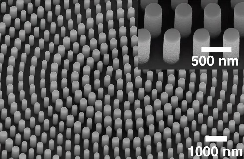
Two studies report new methods for using metasurfaces to create and control dark areas called “optical singularities.”
Optical devices and materials allow scientists and engineers to harness light for research and real-world applications, like sensing and microscopy. Federico Capasso’s group at the Harvard John A. Paulson School of Engineering Applied Sciences (SEAS) has dedicated years to inventing more powerful and sophisticated optical methods and tools. Now, his team has developed new techniques to exert control over points of darkness, rather than light, using metasurfaces.
“Dark regions in electromagnetic fields, or optical singularities, have traditionally posed a challenge due to their complex structures and the difficulty in shaping and sculpting them. These singularities, however, carry the potential for groundbreaking applications in fields such as remote sensing and precision measurement,” said Capasso, the Robert L. Wallace Professor of Applied Physics and Vinton Hayes Senior Research Fellow in Electrical Engineering at SEAS and senior corresponding author on two new papers describing the work.


Crystals that can freely conduct electrons, but not heat, hold great potential for numerous applications. A team of researchers has developed a method for discovering and developing these materials.

The results are published in the Proceedings of the National Academy of Sciences (PNAS).
Unlike glasses, which have very low thermal conductivity, crystals tend to be good conductors of both heat and electrons. There are, however, some that have low thermal conductivity, and the researchers set out to understand the properties of these materials and how they can be developed.

A seemingly magical material can block microwaves, infrared (IR) heat, and light and then magically shift to a transparent state that also allows IR and microwaves to pass through simply by being stretched or contracted.
Inspired by the properties of squid skin, which can shift from translucent to opaque due to the presence of iridocytes and chromatophores, the new material could help create stealth materials, safeguard electronic devices, dramatically improve energy efficiency in commercial buildings, and even protect against microwave weapons.
No One Has Accomplished All of These Feats in One Material .

Topological phases of matter can enable highly stable qubits with small footprints, fast gate times, and digital control. These hardware-protected qubits must be fabricated with a material combination in which a topological phase can reliably be induced. The challenge: disorder can destroy the topological phase and obscure its detection. This paper reports on devices with low enough disorder to pass the topological gap protocol, thereby demonstrating gapped topological superconductivity and paving the way for a new stable qubit.

Diamond has long been the go-to material for quantum sensing due to its coherent nitrogen-vacancy centers, controllable spin, sensitivity to magnetic fields, and ability to be used at room temperature. With such a suitable material so easy to fabricate and scale, there’s been little interest in exploring diamond alternatives.
But this GOAT of the quantum world has one Achilles Heel—It’s too big. Just as an NFL linebacker is not the best sportsperson to ride in the Kentucky Derby, diamond is not an ideal material when exploring quantum sensors and information processing. When diamonds get too small, the super-stable defect it’s renowned for begins to crumble. There is a limit at which diamond becomes useless.
HBN has previously been overlooked as a quantum sensor and a platform for quantum information processing. This changed recently when a number of new defects were discovered that are shaping up to be compelling competitors to diamond’s nitrogen vacancy centers.

The simplicity of the approach stumped even reviewers of the journal Nature and needed further proof to be believed.
Researchers at the College of Chemistry and Molecular Sciences at Wuhan University in China have achieved a significant ‘breakthrough’ in materials science that allows alloys to be made from a diverse range of metals and at much lower temperatures than conventional methods, the South China Morning Post.
Since the Bronze Age, alloys have contributed to the advancement of our civilization. Modern-day applications of alloys involve creating and manufacturing high-entropy alloys (HEAs) composed of five or more metallic elements.