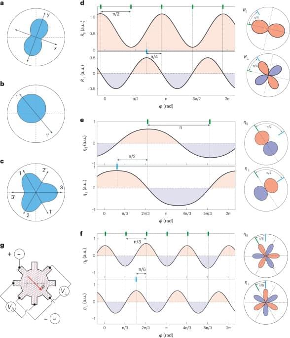
Angle-resolved transport measurements on twisted trilayer graphene reveal evidence for a variety of correlated states with spontaneous symmetry breaking, and offer evidence of momentum polarization.

MIT researchers used ultrathin van der Waals materials to create an electron magnet that can be switched at room temperature. This type of magnet could be used to build magnetic processors or memories that would consume far less energy than silicon devices.
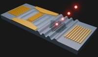
In pursuing quantum networking technologies, single-photon emitters in acoustic cavities are a promising pathway that enables the conversion and transfer of quantum information across multiple platforms. The recent discovery of single-photon emitters within two-dimensional (2D) materials, such as WSe and hexagonal boron nitride (h-BN), opens new avenues in exploring such quantum optomechanical phenomena in lower dimensional systems. In this work, we demonstrate the integration of 2D-based single-photon emitters with surface acoustic wave optomechanical cavities and illustrate their potential for radio-frequency electronic control of quantum light emission.
Using simple exfoliation techniques, WSe and h-BN layers are transferred onto surface acoustic wave cavities patterned on lithium niobate—a highly piezoelectric host material. Using electro-optical measurements, we confirm high-quality resonators and cavity-phonon modes that couple to the 2D quantum emitters. Remarkably, the interaction between the 2D emitters and acoustic waves is exceptionally strong owing to the ultrathin nature of the 2D materials and their proximity to the surface waves, verified through quantum spectroscopy measurements. In addition to the radio-frequency acoustic modulation of the emitters in these materials, new physics emerges from the emitter-phonon coupling that leads to new mechanisms for high-speed manipulation of quantum emitters, opening avenues for the generation of entangled-photon pairs.
These advancements set the stage for the exploration of cavity optomechanics with 2D materials. In future experiments, higher frequency resonators will enable studies of the interplay and dynamics between single photons and phonons deep in the quantum regime, a key technology for quantum networking.
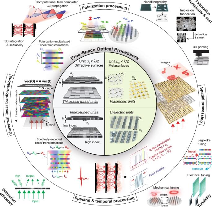
Optica l computing via free-space-based structured optical materials allows to access optical information without the need for preprocessing or optoelectronic conversion. In this Perspective, the authors describe opportunities and challenges in their use for optical computing, information processing, computational imaging and sensing.

Directing magnetization with a low electric field is crucial for advancing effective spintronic devices. In spintronics, the characteristics of an electron’s spin or magnetic moment are leveraged for information storage. By modifying orbital magnetic moments through strain, it’s possible to manipulate electron spins, leading to an enhanced magnetoelectric effect for superior performance.
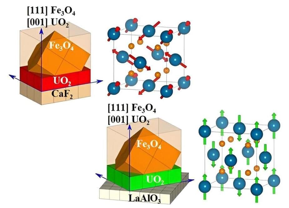
Japanese researchers, including Jun Okabayashi from the University of Tokyo, revealed a strain-induced orbital control mechanism in interfacial multiferroics. In multiferroic material, the magnetic property can be controlled using an electric field—potentially leading to efficient spintronic devices. The interfacial multiferroics that Okabayashi and his colleagues studied consist of a junction between a ferromagnetic material and a piezoelectric material. The direction of magnetization in the material could be controlled by applying voltage.
Electronics are based on electrical charges being transported from one place to another. Electrons move, current flows, and signals are transmitted by applying an electrical voltage. However, there is also another way to manipulate electronic currents and signals: using the properties of the spin—the intrinsic magnetic moment of the electron. This is called “spintronics,” and it has become an increasingly important field in contemporary electronic research.
An international research team involving TU Wien and the Czech Academy of Sciences has now achieved an important breakthrough. They have managed to switch the spins in an antiferromagnetic material using surface strain. This could lead to an important new line of research in electronic technologies. The research is published in the journal Advanced Functional Materials.
“There are different types of magnetism,” explains Sergii Khmelevskyi from the Vienna Scientific Cluster Research Center, TU Wien. “The best known is ferromagnetism. It occurs when the atomic spins in a material are all aligned in parallel. But there is also the opposite, antiferromagnetism. In an antiferromagnetic material, neighboring atoms always have opposite spins.” Their effects therefore cancel each other out and no magnetic force can be detected from the outside.
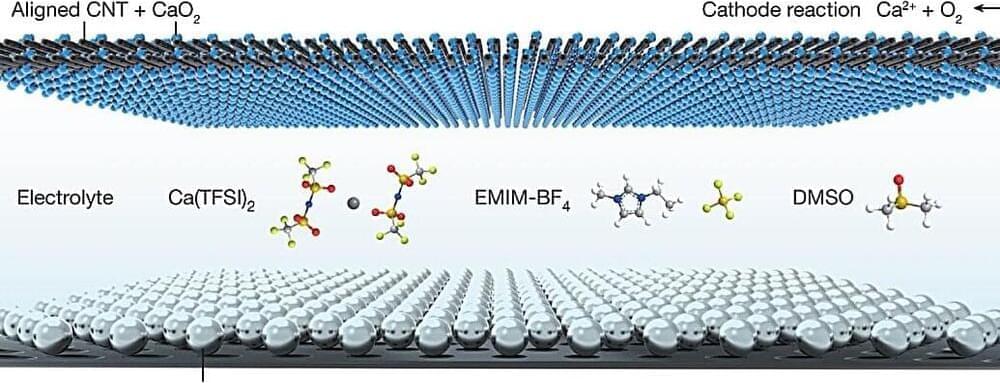
A multi-institutional team of Chinese engineers has developed a proof-of-concept calcium-based battery that withstands 700 charge cycles at room temperature. In their paper published in the journal Nature, the group describes the challenges they addressed in developing the battery and what they have learned about the possible use of calcium-based batteries in consumer products in the future.
The current standard for rechargeable batteries used in consumer products is lithium. But because it is a rare material and has issues such as poor aging and the need to prevent overcharge, scientists have been looking for a suitable replacement. One such material is calcium, which is 2,500 times as abundant as lithium.
Prior research has suggested rechargeable batteries based on calcium should be possible if problems can be resolved. One of the biggest challenges is finding suitable electrolyte and electrode materials that can provide stability and safety.
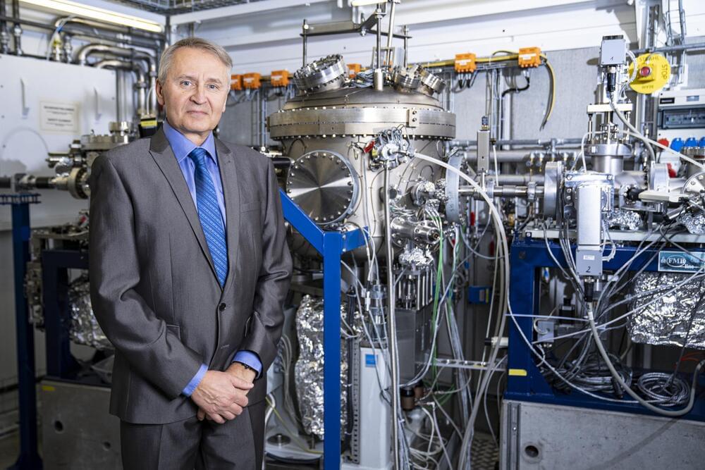
There is now a new addition to the magnetic family: thanks to experiments at the Swiss Light Source SLS, researchers have proved the existence of altermagnetism. The experimental discovery of this new branch of magnetism is reported in Nature and signifies new fundamental physics, with major implications for spintronics.
Magnetism is a lot more than just things that stick to the fridge. This understanding came with the discovery of antiferromagnets nearly a century ago. Since then, the family of magnetic materials has been divided into two fundamental phases: the ferromagnetic branch known for several millennia and the antiferromagnetic branch.
The experimental proof of a third branch of magnetism, termed altermagnetism, was made at the Swiss Light Source SLS, by an international collaboration led by the Czech Academy of Sciences together with Paul Scherrer Institute PSI.

The lunar sample returned by China’s 2020 lunar mission contained minerals that provide clues to their origin. China’s Chang’e-5, the first lunar sample return mission since the Soviet Union’s Luna 24 in 1976, delivered 1.73 kilograms of regolith from the Oceanus Procellarum, a plane named for its vast size. The sample landed with CE-5 in late 2020 and included a new mineral, Changesite-(Y), as well as a perplexing combination of silica minerals. Researchers now compare CE-5’s material composition to other lunar and Martian regolith samples and examine potential causes and origins for the lunar sample’s unique makeup.
Earth’s moon achieved its Swiss cheese appearance from celestial objects crashing into its surface, forming impact craters. But craters weren’t all that was left behind; the intense pressure and temperature of such a collision also impacts the rocks and dust covering the lunar surface, known as regolith, altering its mineral composition and structure. Analyzing the resulting minerals provides modern researchers clues to the moon’s past.
China’s Chang’e-5, the first lunar sample return mission since the Soviet Union’s Luna 24 in 1976, delivered 1.73 kilograms of regolith from the Oceanus Procellarum, a plane named for its vast size.
