Toggle light / dark theme

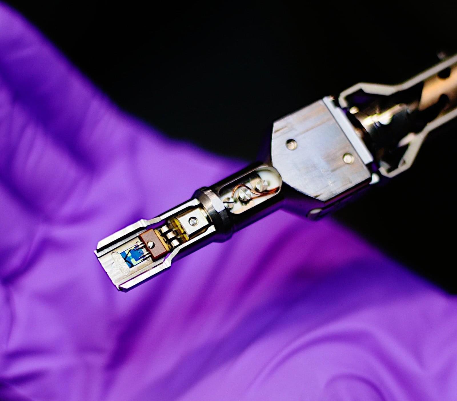
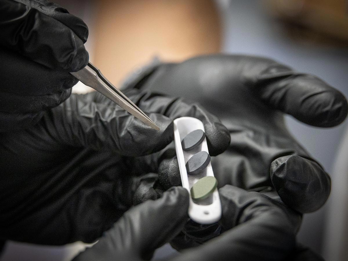
Ingestible devices are often used to study and treat hard-to-reach tissues in the body. Swallowed in pill form, these capsules can pass through the digestive tract, snapping photos or delivering drugs.

While in their simplest form, these devices are passively transported through the gut, there are a wide range of applications where you may want a device to attach to the tissue or other flexible materials. A rich history of biologically inspired solutions exist to address this need, ranging from cocklebur-inspired Velcro to slug-inspired medical adhesives, but the creation of on-demand and reversible attachment mechanisms that can be incorporated into millimeter-scale devices for biomedical sensing and diagnostics remains a challenge.

A new interdisciplinary effort led by Robert Wood, the Harry Lewis and Marlyn McGrath Professor of Engineering and Applied Sciences in the Harvard John A. Paulson School of Engineering and Applied Sciences (SEAS), and James Weaver, of Harvard’s Wyss Institute, has drawn inspiration from an unexpected source: the world of parasites.

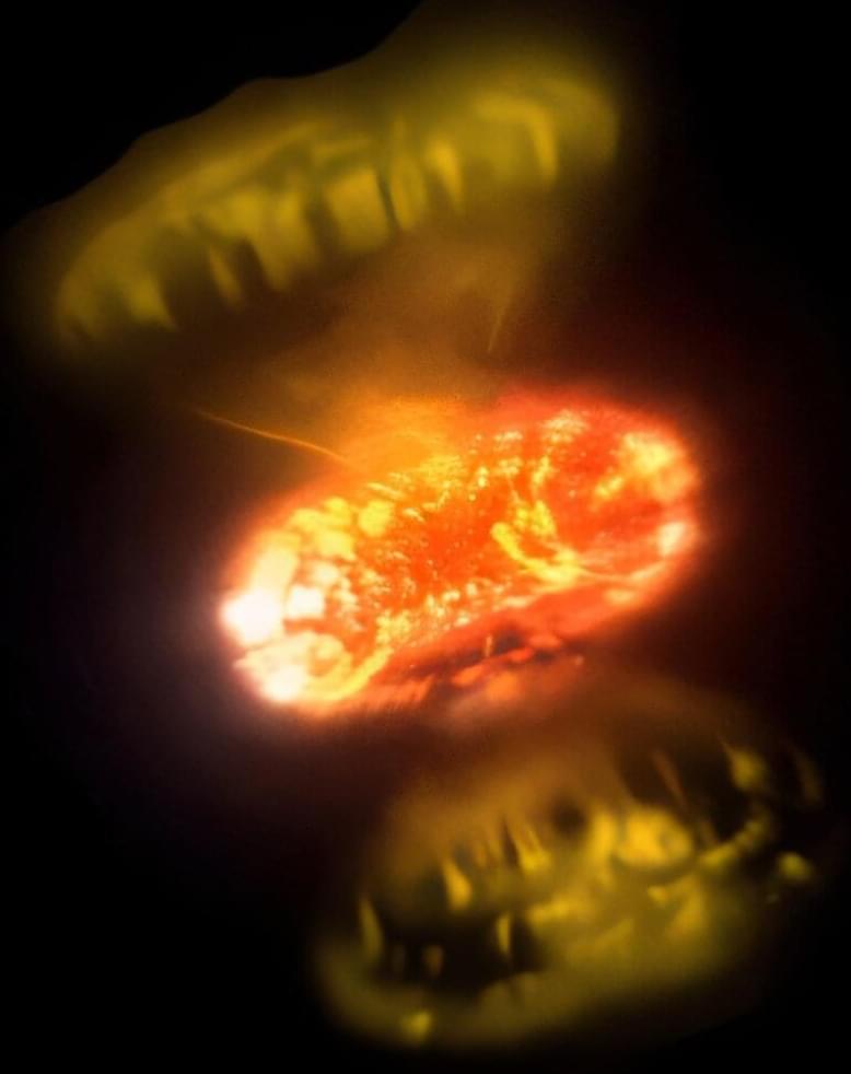
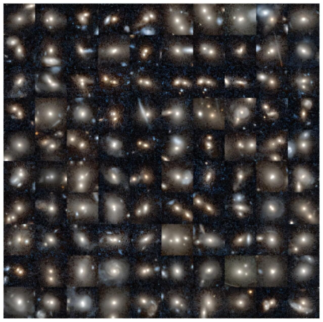
Astronomers have used the unique capabilities of NASA’s Hubble Space Telescope to peer closer than ever into the throat of an energetic monster black hole powering a quasar. A quasar is a galactic center that glows brightly as the black hole consumes material in its immediate surroundings.

The new Hubble views of the environment around the quasar show a lot of “weird things,” according to Bin Ren of the Côte d’Azur Observatory and Université Côte d’Azur in Nice, France. “We’ve got a few blobs of different sizes, and a mysterious L-shaped filamentary structure. This is all within 16,000 light-years of the black hole.”

Some of the objects could be small satellite galaxies around the black hole, and so they could offer the materials that will accrete onto the central super massive black hole, powering the bright lighthouse.

A method that can grow a useful insulating material into exceptionally high-quality films that are just one atom thick and are suitable for industrial-scale production has been developed by an international team led by Xixiang Zhang from KAUST.

The work is published in the journal Nature Communications.

The material, called (hBN), is used in and can also enhance the performance of other two-dimensional (2D) materials such as graphene and transition metal dichalcogenides (TMDs).

Transistors based on two-dimensional (2D) semiconductors, such as molybdenum disulfide (MoS2) and tungsten diselenide (WSe2), could outperform conventional silicon-based transistors, while also being easier to reduce in size. To perform well, these transistors need to be based on high-quality dielectric materials, which can be difficult to prepare.

Researchers at Nanyang Technological University, Nanjing University of Aeronautics and Astronautics recently introduced a new promising strategy to prepare the dielectric materials for these transistors. Their approach, outlined in a paper published in Nature Electronics, was successfully used to deposit an ultrathin and uniform native oxide of Ga2O3 on the surface of MoS2.

“Traditional methods of preparing dielectric layer, such as (ALD), encounter quality problems because of the high-quality surface of 2D semiconductors without sufficient nucleation points, especially at thin thicknesses down to a few nanometers,” Kongyang Yi, first author of the paper, told Tech Xplore.

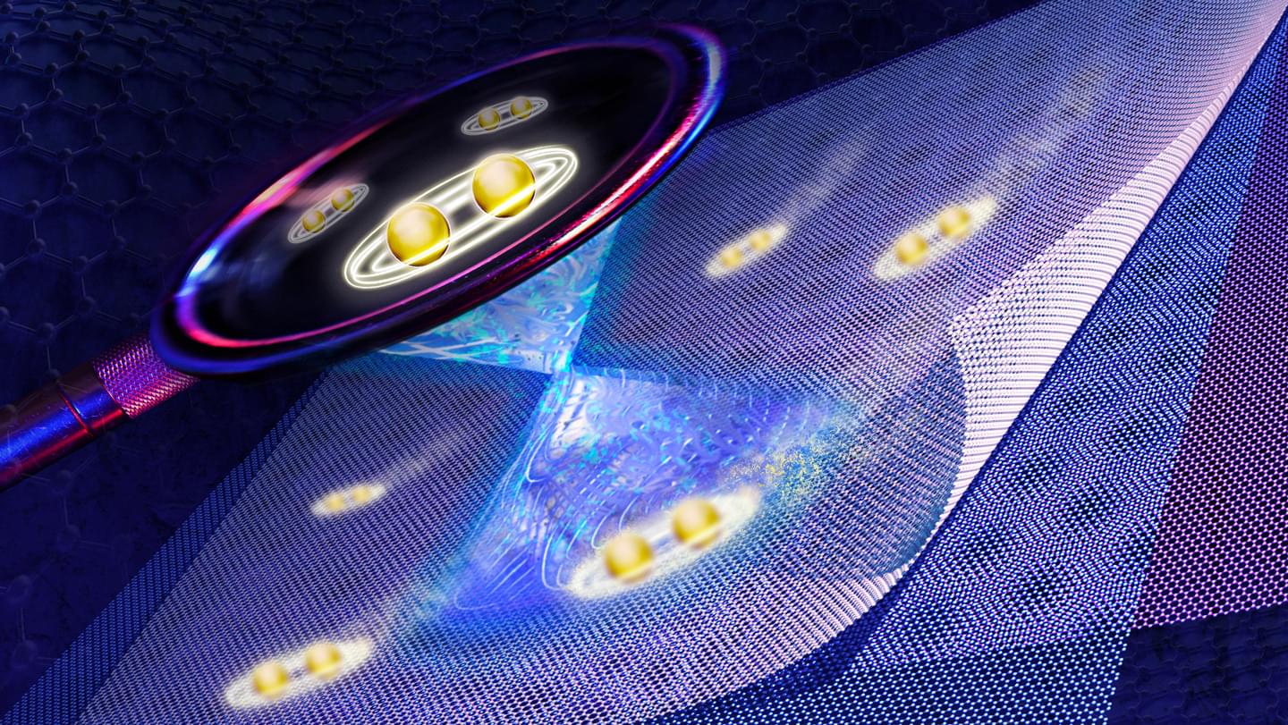
An international research team has for the first time designed realistic photonic time crystals–exotic materials that exponentially amplify light. The breakthrough opens up exciting possibilities across fields such as communication, imaging and sensing by laying the foundations for faster and more compact lasers, sensors and other optical devices.

“This work could lead to the first experimental realization of photonic time crystals, propelling them into practical applications and potentially transforming industries. From high-efficiency light amplifiers and advanced sensors to innovative laser technologies, this research challenges the boundaries of how we can control the light-matter interaction,” says Assistant Professor Viktar Asadchy from Aalto University, Finland.

The study is published in the journal Nature Photonics.

We’ve all experienced the moment of panic when a glass slips from our hands, shattering into pieces upon hitting the ground. What if this common mishap could become a thing of the past?

Now, a new discovery by researchers at Tohoku University has offered insights into how resists breakage, potentially paving the way for highly durable, break-resistant materials. The breakthrough has wide ranging implications for glass-related industries.

Details of their findings are published in the journal Acta Materialia.

The ability to control and optimize electron behavior is crucial for realizing the potential of the best quantum materials.


Scientists at Loughborough University have made an exciting breakthrough in understanding how fine-tuning the behavior of electrons in quantum materials can unlock the next generation of advanced technologies.

A new technique employing monochromatic light improves the study of internal structures in materials affected by light scattering, enabling detailed observation of particle concentrations.

When driving through a bank of fog, car headlights are only moderately helpful since the light is scattered by the water particles suspended in the air. A similar situation occurs when trying to observe the inside of a drop of milk in water or the internal structure of an opal gem with white light. In these cases, multiple light scattering effects prevent examination of the interior.

Now, a team of researchers at Johannes Gutenberg University Mainz (JGU) and Heinrich Heine University Düsseldorf (HHU) has overcome this challenge and developed a new method to study the interior of a crystalline drop.