Toggle light / dark theme

One of the cornerstones of the implementation of quantum technology is the creation and manipulation of the shape of external fields that can optimize the performance of quantum devices. Known as quantum optimal control, this set of methods comprises a field that has rapidly evolved and expanded over recent years.

A new review paper published in EPJ Quantum Technology and authored by Christiane P. Koch, Dahlem Center for Complex Quantum Systems and Fachbereich Physik, Freie Universität Berlin along with colleagues from across Europe assesses recent progress in the understanding of the controllability of quantum systems as well as the application of quantum control to quantum technologies. As such, it lays out a potential roadmap for future .

While quantum optimal control builds on conventional control theory encompassing the interface of applied mathematics, engineering, and physics, it must also factor in the quirks and counter-intuitive nature of quantum physics.

How expensive is it to make a panel that uses e-ink technology? That might depend on how flexible you are. [RBarron] read about reverse engineering point-of-sale shelf labels and found them on eBay for just over a buck apiece. Next thing you know, 20 of them were working together in a single panel.

The panels use RF or NFC programming, normally, but have the capability to use BLE. Naturally you could just address each one in turn, but that isn’t very efficient. The approach here is to use one label as a BLE controller and it then drives the other displays in a serial daisy chain, where each label’s receive pin is set to the previous label’s transmit pin.

Innovative Solutions For Unmet Needs Of Older Adults & Their Caregivers — Keith Camhi, Managing Director, Techstars Future of Longevity Accelerator — A Partnership With Melinda Gates Pivotal Ventures.


Keith Camhi is Managing Director, Techstars Future of Longevity Accelerator (https://www.techstars.com/accelerators/longevity), a program, run in partnership with Pivotal Ventures (https://www.pivotalventures.org/), an investment and incubation company created by Melinda French Gates, focusing on innovative solutions to address the unmet needs of older adults and their caregivers. The longevity accelerator core program themes include: Caregiver Support, Care Coordination, Aging in Place, Financial Wellness and Resilience, Preventive Health (both Physical and Cognitive), and Social Engagement.

Keith was previously the SVP of Accelerators for Techstars globally and was inspired to move to the MD role for the longevity program based on having built a venture-backed startup serving older adults himself, having experienced the gaps in America’s care giving infrastructure firsthand, and wanting to support entrepreneurs who are building solutions to address this substantial market opportunity.

Researchers at the University of Massachusetts Amherst and the Georgia Institute of Technology have 3D printed a dual-phase, nanostructured high-entropy alloy that exceeds the strength and ductility of other state-of-the-art additively manufactured materials, which could lead to higher-performance components for applications in aerospace, medicine, energy and transportation.

The work, led by Wen Chen, assistant professor of mechanical and industrial engineering at UMass, and Ting Zhu, professor of mechanical engineering at Georgia Tech, is published by the journal Nature (“Strong yet ductile nanolamellar high-entropy alloys by additive manufacturing”).

Wen Chen, assistant professor of mechanical and industrial engineering at UMass Amherst, stands in front of images of 3D printed high-entropy alloy components (heatsink fan and octect lattice, left) and a cross-sectional electron backscatter diffraction inverse-pole figure map demonstrating a randomly oriented nanolamella microstructure (right). (Image: UMass Amherst)

Quantum computing, though still in its early days, has the potential to dramatically increase processing power by harnessing the strange behavior of particles at the smallest scales. Some research groups have already reported performing calculations that would take a traditional supercomputer thousands of years. In the long term, quantum computers could provide unbreakable encryption and simulations of nature beyond today’s capabilities.

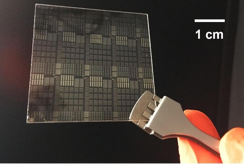
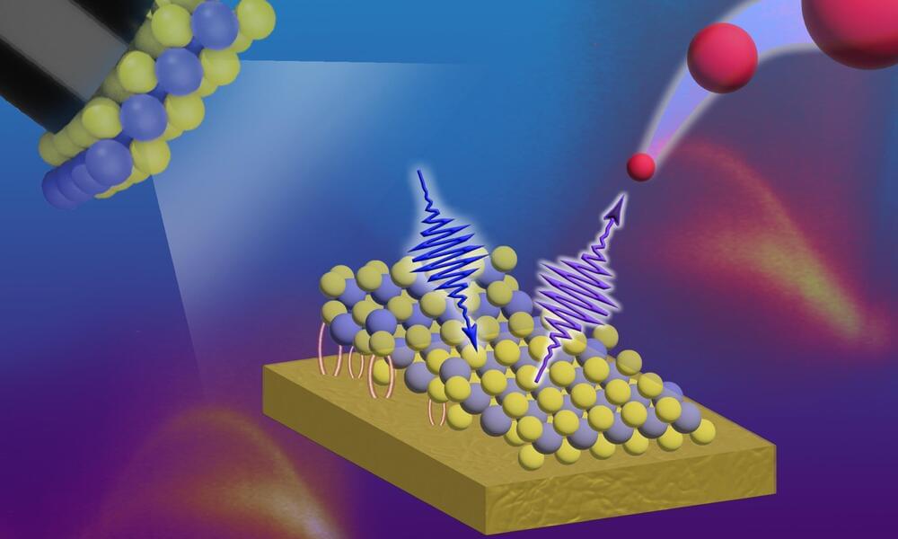
A UCLA-led interdisciplinary research team including collaborators at Harvard University has now developed a fundamentally new strategy for building these computers. While the current state of the art employs circuits, semiconductors and other tools of electrical engineering, the team has produced a game plan based in chemists’ ability to custom-design atomic building blocks that control the properties of larger molecular structures when they’re put together.

The findings, published last week in Nature Chemistry, could ultimately lead to a leap in quantum processing power.

Researchers have reported the discovery of an exoplanet orbiting Ross 508 near the inner edge of its habitable zone.


Researchers at the University of Massachusetts Amherst recently announced that they have figured out how to engineer a biofilm that harvests the energy in evaporation and converts it to electricity. This biofilm, which was announced in Nature Communications, has the potential to revolutionize the world of wearable electronics, powering everything from personal medical sensors to personal electronics.

“This is a very exciting technology,” says Xiaomeng Liu, graduate student in electrical and computer engineering in UMass Amherst’s College of Engineering and the paper’s lead author. “It is real green energy, and unlike other so-called ‘green-energy’ sources, its production is totally green.”

That’s because this —a thin sheet of bacterial cells about the thickness of a sheet of paper—is produced naturally by an engineered version of the bacteria Geobacter sulfurreducens. G. sulfurreducens is known to produce electricity and has been used previously in “microbial batteries” to . But such batteries require that G. sulfurreducens is properly cared for and fed a constant diet. By contrast, this new biofilm, which can supply as much, if not more, energy than a comparably sized battery, works, and works continuously, because it is dead. And because it’s dead, it doesn’t need to be fed.

Scientists at the Lawrence Livermore National Laboratory (LLNL) Energetic Materials Center and Purdue University Materials Engineering Department have used simulations performed on the LLNL supercomputer Quartz to uncover a general mechanism that accelerates chemistry in detonating explosives critical to managing the nation’s nuclear stockpile. Their research is featured in the July 15 issue of the Journal of Physical Chemistry Letters.

Insensitive high explosives based on TATB (1,3,5-triamino-2,4,6-trinitrobenzene) offer enhanced safety properties over more conventional explosives, but physical explanations for these safety characteristics are not clear. Explosive initiation is understood to arise from hotspots that are formed when a shockwave interacts with microstructural defects such as pores. Ultrafast compression of pores leads to an intense localized spike in temperature, which accelerates chemical reactions needed to initiate burning and ultimately . Engineering models for insensitive high explosives—used to assess safety and performance—are based on the hotspot concept but have difficulty in describing a wide range of conditions, indicating missing physics in those models.

Using large-scale atomically resolved reactive molecular dynamics supercomputer simulations, the team aimed to directly compute how hotspots form and grow to better understand what causes them to react.

The startup is hiring Ritesh Jain, VP of engineering at Intel, to help it move from the prototype phase of its chip development to mass production.


ESA is prepping to send a spacecraft to Venus — a feat which will require state-of-the-art methods to get through the planet’s grueling atmosphere.

The subtractive manufacturing process involves etching, drilling, or cutting from a solid board to build the final product. It is ideal for applications using a wide variety of materials and in the PCB fabrication of large-size products. In the additive manufacturing process, a product is developed by adding material one layer at a time and bonding the layers together until the final product is ready. The ability to control material density and the possibility of including intricate features makes this process versatile. It is used in a range of engineering and manufacturing applications, especially in custom manufacturing.

Benefits of 3D printing in medical device manufacturing.

3D printing is economical and offers quick PCB prototyping without the need for complex manufacturing steps. It optimizes the PCB design process by avoiding possible design faults in the initial PCB design stages. 3D printing is easy on flex PCBs and multilayer PCB printing is possible using the latest design software. With the growing manufacturing trends and improving software, 3D printing will be more than a prototyping tool and can be a viable alternative for production parts. 3D printing has been recently used for the end-part manufacturing of several medical devices like hearing aids, dental implants, and more. It is more beneficial for low-volume productions.