Toggle light / dark theme

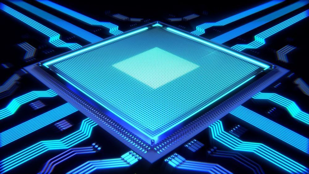
IBM, its Research Alliance partners Globalfoundries and Samsung, and equipment suppliers have developed an industry-first process to build silicon nanosheet transistors that will enable 5 nanometer (nm) chips. The details of the process will be presented at the 2017 Symposia on VLSI Technology and Circuits conference in Kyoto, Japan. In less than two years since developing a 7nm test node chip with 20 billion transistors, scientists have paved the way for 30 billion switches on a fingernail-sized chip.

The resulting increase in performance will help accelerate cognitive computing, the Internet of Things (IoT), and other data-intensive applications delivered in the cloud. The power savings could also mean that the batteries in smartphones and other mobile products could last two to three times longer than today’s devices, before needing to be charged.

Scientists working as part of the IBM-led Research Alliance at the SUNY Polytechnic Institute Colleges of Nanoscale Science and Engineering’s NanoTech Complex in Albany, NY achieved the breakthrough by using stacks of silicon nanosheets as the device structure of the transistor, instead of the standard FinFET architecture, which is the blueprint for the semiconductor industry up through 7nm node technology.

Read more

Tibetan singing bowl (credit: Baycrest Health Sciences)

A study by neuroscientists at Toronto-based Baycrest Rotman Research Institute and Stanford University involving playing a musical instrument suggests ways to improve brain rehabilitation methods.

In the study, published in the Journal of Neuroscience on May 24, 2017, the researchers asked young adults to listen to sounds from an unfamiliar musical instrument (a Tibetan singing bowl). Half of the subjects (the experimental group) were then asked to recreate the same sounds and rhythm by striking the bowl; the other half (the control group) were instead asked to recreate the sound by simply pressing a key on a computer keypad.

Read more

A mantra of these data-rife times is that within the vast and growing volumes of diverse data types, such as sensor feeds, economic indicators, and scientific and environmental measurements, are dots of significance that can tell important stories, if only those dots could be identified and connected in authentically meaningful ways. Getting good at that exercise of data synthesis and interpretation ought to open new, quicker routes to identifying threats, tracking disease outbreaks, and otherwise answering questions and solving problems that previously were intractable.

Now for a reality check. “Today’s hardware is ill-suited to handle such data challenges, and these challenges are only going to get harder as the amount of data continues to grow exponentially,” said Trung Tran, a program manager in DARPA’s Microsystems Technology Office (MTO). To take on that technology shortfall, MTO last summer unveiled its Hierarchical Identify Verify Exploit (HIVE) program, which has now signed on five performers to carry out HIVE’s mandate: to develop a powerful new data-handling and computing platform specialized for analyzing and interpreting huge amounts of data with unprecedented deftness. “It will be a privilege to work with this innovative team of performers to develop a new category of server processors specifically designed to handle the data workloads of today and tomorrow,” said Tran, who is overseeing HIVE.

The quintet of performers includes a mix of large commercial electronics firms, a national laboratory, a university, and a veteran defense-industry company: Intel Corporation (Santa Clara, California), Qualcomm Intelligent Solutions (San Diego, California), Pacific Northwest National Laboratory (Richland, Washington), Georgia Tech (Atlanta, Georgia), and Northrop Grumman (Falls Church, Virginia).

Read more

The smallest and most advanced chips currently commercially available are made up of transistors with gates about 10 nm long, but IBM has now unveiled plans to cut them in half. To create 5 nm chips, the company is ditching the standard FinFET architecture in favor of a new structure built with a stack of four nanosheets, allowing some 30 billion transistors to be packed onto a chip the size of a fingernail and promising significant gains in power and efficiency.

First coined in the 1970s, Moore’s Law was the observation that the number of transistors on a single chip would double every two years. The trend has held up pretty well ever since, but the time frame of the doubling has slowed down a little in recent years. In consumer electronics, 14 nm chips are still stock-standard, but advances from the likes of Intel and Samsung mean that 10 nm versions have started hitting the high-end market.

Read more

Please enjoy this interview with Dr. Aubrey de Grey, Chief Science Officer and Co-founder of SENS Research Foundation — one of the most successful advocacy and fundraising initiatives supporting breakthrough research on the main mechanisms of aging and age-related diseases. http://www.sens.org

In this video Dr. de Grey speaks about the progress in developing interventions to tackle age-related damages identified by SENS as the main ones.

Interviewer — LEAF/Lifespan.io Board member Elena Milova.

Dr. de Grey received his BA in Computer Science and Ph.D. in Biology from the University of Cambridge in 1985 and 2000, respectively. He is Editor-in-Chief of Rejuvenation Research (http://www.liebertpub.com/overview/rejuvenation-research/127/), is a Fellow of both the Gerontological Society of America and the American Aging Association, and sits on the editorial and scientific advisory boards of numerous journals and organizations.

Implants, transhumanism, & the US Navy in this new article: http://akashictimes.co.uk/brits-line-up-to-be-microchipped/ #transhumanism #implants


Is this the mark of the beast?

A growing number of people in the UK are getting microchipped, according to new findings.

The BBC recently featured video stories from a number of people – some of them from Leeds – who call themselves “bio-hackers”.

Intel announced a new family of “Core X” desktop processors at Computex today, offering even more powerful versions of its existing Core i5 and Core i7 models, along with a new, top-of-the-line Core i9 line for those who want even more firepower.

The Core X platform is being targeted squarely at enthusiast customers like gamers and content creators — people who want to be able to run the latest games at the best possible resolution while streaming footage and running a chat with viewers or have four different creative tools open at once to put together a new vlog.

To that end, the Core X-series scales from models with 4-cores topping out with the $1,999 Core i9 Extreme, which Intel proudly points out is the first consumer desktop processor to offer 18-cores and 36-threads.

Read more

Over the past 40 years, microelectronics have advanced by leaps and bounds thanks to silicon and complementary metal-oxide semiconductor (CMOS) technology, enabling computing, smartphones, compact and low-cost digital cameras, as well as most of the electronic gadgets we rely on today.

However, the diversification of this platform into applications other than microcircuits and visible light cameras has been impeded by the difficulty of combining non-silicon semiconductors with CMOS.

IFCO researchers have now overcome this obstacle, showing for the first time the monolithic integration of a CMOS integrated circuit with graphene, resulting in a high-resolution consisting of hundreds of thousands of photodetectors based on graphene and quantum dots (QD). They incorporated it into a digital camera that is highly sensitive to UV, visible and infrared light simultaneously. This has never before been achieved with existing imaging sensors. In general, this demonstration of monolithic integration of graphene with CMOS enables a wide range of optoelectronic applications, such as low-power optical data communications and compact and ultra sensitive sensing systems.

Read more