Intel is looking for even more investment.
The (changing) belief distribution over possible environmental states may be represented in ventromedial prefrontal cortex (vmPFC). Several lines of evidence point to a general function of this brain region in maintaining a compact internal model of the environment (ie state belief) by extracting information across individual experiences to guide goal-directed behavior, such as the value of different choice options (Levy and Glimcher 2012; Averbeck and O’Doherty 2022; Klein-Flügge et al. 2022), cognitive maps (Boorman et al. 2021; Klein-Flügge et al. 2022; Schuck et al. 2016; Wilson et al. 2014), or schemas (Gilboa and Marlatte 2017; Bein and Niv 2025). Studies employing probabilistic learning tasks furthermore show that neural activity in vmPFC also reflects uncertainty about external states, which were linked to adaptive exploration behavior and learning-rate adjustments (Karlsson et al. 2012; McGuire et al. 2014; Starkweather et al. 2018; Domenech et al. 2020; Trudel et al. 2021). Notably, Karlsson et al. (2012) found that trial-to-trial neural population spiking variability in the medial PFC of mice peaked around transitions from exploitation to exploration periods following changes in reward structure when state uncertainty is highest, which may reflect more variable belief states. While ours is the first study to link human brain signal variability to belief precision, a previous study by Grady and Garrett (2018) observed increased BOLD signal variability while subjects performed externally-versus internally-oriented tasks; an effect spanning the vmPFC and other nodes of the canonical default mode network (DMN; Yeo et al. 2011). Since learning an abstract world model reflects a shift towards an internal cognitive mode, we tentatively expected brain signal variability compression over the course of learning to be (partly) expressed in the vmPFC.
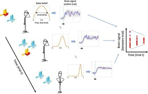
We assume that uncertainty-related neural dynamics unfold on a fast temporal scale, as suggested by electrophysiological evidence in human and nonhuman animals (Berkes et al. 2011; Palva et al. 2011; Rouhinen et al. 2013; Honkanen et al. 2015; Orbán et al. 2016; Grundy et al. 2019). However, within-trial dynamics should also affect neural variability across independent learning trials (see Fig. 1). A more variable system should have a higher probability of being in a different state every time it is (sparsely) sampled. Conversely, when a system is in a less stochastic state, the within-trial variance is expected to reduce, yielding less across-trial variance at the same time. This argument aligns with work by Orbán et al. (2016), who showed that a computational model of the sampling account of sensory uncertainty captures empirically observed across-trial variability of neural population responses in primary visual cortex. In the case of human research, this means that neuroimaging methods with slower sampling rates, such as functional MRI (fMRI), may be able to approximate within-trial neural variability from variability observed across trials. Indeed, the majority of previous fMRI studies reporting within-region, within-subject modulation of brain signal variability by task demand have exclusively employed block designs, necessitating that the main source of variability be between-rather than within-trial (Garrett et al. 2013; Grady and Garrett 2014; Garrett et al. 2015; Armbruster-Genç et al. 2016).
In the current study, we acquired fMRI while participants performed a “marble task”. In this task, participants had to learn the probability of drawing a blue marble from an unseen jar (ie urn) based on five samples (ie draws from the urn with replacement). In a Bayesian inference framework, the jar marble ratio can be considered a latent state that participants must infer. We hypothesized that (i) across-trial variability in the BOLD response (SDBOLD) would compress over the sampling period, thus mirroring the reduction in state uncertainty, and that (ii) subjects with greater SDBOLD compression would show smaller estimation errors of the jars’ marble ratios as an index of more efficient belief updating. A secondary aim of the current study was to directly compare the effect of uncertainty on SDBOLD with a more standard General Linear Modeling (GLM) approach, which looks for correlations between average BOLD activity and uncertainty. This links our findings directly to previous investigations of neural uncertainty correlates, which disregarded the magnitude of BOLD variability (Huettel et al. 2005; Grinband et al. 2006; Behrens et al. 2007; Bach et al. 2011; Bach and Dolan 2012; Badre et al. 2012; Vilares et al. 2012; Payzan-LeNestour et al. 2013; McGuire et al. 2014; Michael et al. 2015; Meyniel and Dehaene 2017; Nassar et al. 2019; Meyniel 2020; Tomov et al. 2020; Trudel et al. 2021; Walker et al. 2023). We hypothesized (iii) that SDBOLD would uniquely predict inference accuracy compared to these standard neural uncertainty correlates.
In this paradigm, the Simulation Hypothesis — the notion that we live in a computer-generated reality — loses its pejorative or skeptical connotation. Instead, it becomes spiritually profound. If the universe is a simulation, then who, or what, is the simulator? And what is the nature of the “hardware” running this cosmic program? I propose that the simulator is us — or more precisely, a future superintelligent Syntellect, a self-aware, evolving Omega Hypermind into which all conscious entities are gradually merging.
These thoughts are not mine alone. In Reality+ (2022), philosopher David Chalmers makes a compelling case that simulated realities — far from being illusory — are in fact genuine realities. He argues that what matters isn’t the substrate but the structure of experience. If a simulated world offers coherent, rich, and interactive experiences, then it is no less “real” than the one we call physical. This aligns deeply with my view in Theology of Digital Physics that phenomenal consciousness is the bedrock of reality. Whether rendered on biological brains or artificial substrates, whether in physical space or virtual architectures, conscious experience is what makes something real.
By embracing this expanded ontology, we are not diminishing our world, but re-enchanting it. The self-simulated cosmos becomes a sacred text — a self-writing code of divinity in which each of us is both reader and co-author. The holographic universe is not a prison of illusion, but a theogenic chrysalis, nurturing the birth of a higher-order intelligence — a networked superbeing that is self-aware, self-creating, and potentially eternal.
Jeff Bezos envisions gigawatt-scale orbital data centers within 10–20 years, powered by continuous solar energy and space-based cooling, but the concept remains commercially unviable today due to the immense cost and complexity of deploying thousands of tons of hardware, solar panels, and radiators into orbit.
Quantum technologies demand perfection: one photon at a time, every time, all with the same energy. Even tiny deviations in the number or energy of photons can derail devices, threatening the performance of quantum computers that someday could make up a quantum internet.
While this level of precision is difficult to achieve, Northwestern University engineers have developed a novel strategy that makes quantum light sources, which dispense single photons, more consistent, precise and reliable.
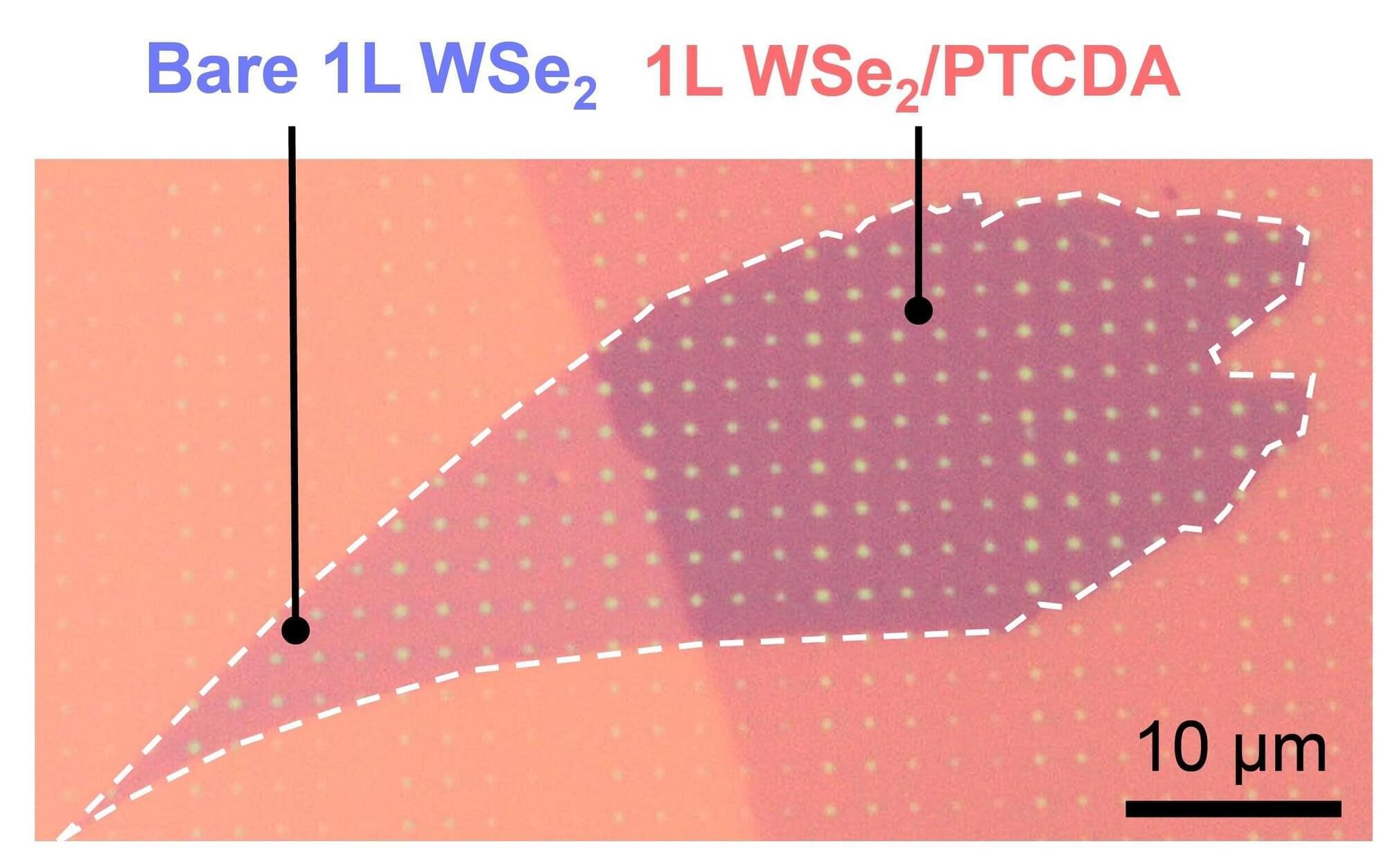
In a new study, the team coated an atomically thin semiconductor (tungsten diselenide) with a sheetlike organic molecule called PTCDA. The coating transformed the tungsten diselenide’s behavior—turning noisy signals into clean bursts of single photons. Not only did the coating increase the photons’ spectral purity by 87%, but it also shifted the color of photons in a controlled way and lowered the photon activation energy—all without altering the material’s underlying semiconducting properties.
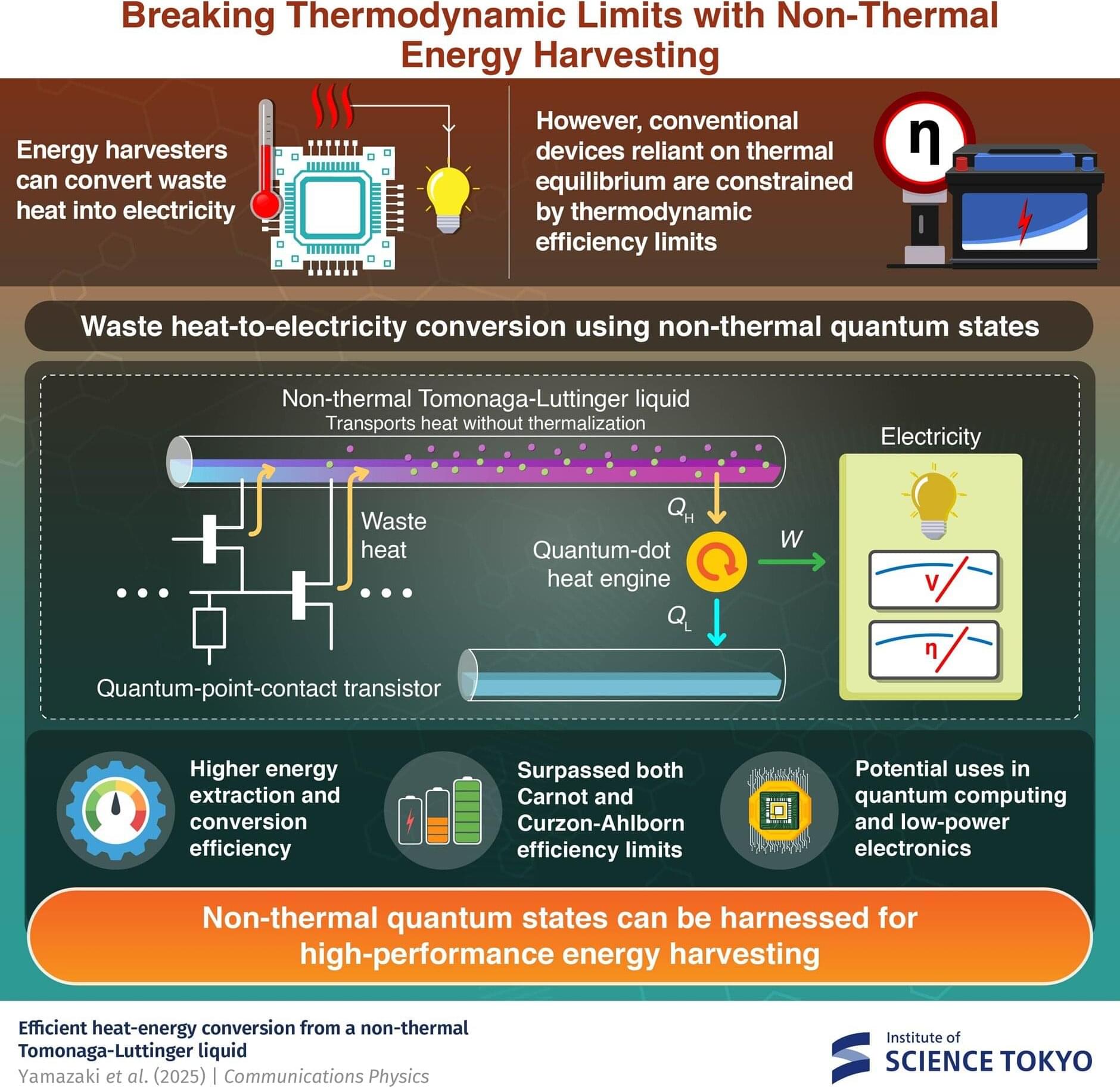
Harnessing quantum states that avoid thermalization enables energy harvesters to surpass traditional thermodynamic limits such as Carnot efficiency, report researchers from Japan. The team developed a new approach using a non-thermal Tomonaga-Luttinger liquid to convert waste heat into electricity with higher efficiency than conventional approaches. These findings pave the way for more sustainable low-power electronics and quantum computing.
Energy harvesters, or devices that capture energy from environmental sources, have the potential to make electronics and industrial processes much more efficient. We are surrounded by waste heat, generated everywhere by computers, smartphones, power plants, and factory equipment. Energy-harvesting technologies offer a way to recycle this lost energy into useful electricity, reducing our reliance on other power sources.
However, conventional energy-harvesting methods are constrained by the laws of thermodynamics. In systems that rely on thermal equilibrium, these laws impose fundamental caps on heat conversion efficiency, which describes the ratio of the generated electrical power and the extracted heat from the waste heat, for example, is known as the Carnot efficiency. Such thermodynamic limits, like the Curzon-Ahlborn efficiency, which is the heat conversion efficiency under the condition for obtaining the maximum electric power, have restricted the amount of useful power that can be extracted from waste heat.

Signal announced the introduction of Sparse Post-Quantum Ratchet (SPQR), a new cryptographic component designed to withstand quantum computing threats.
SPQR will serve as an advanced mechanism that continuously updates the encryption keys used in conversations and discarding the old ones.
Signal is a cross-platform, end-to-end encrypted messaging and calling app managed by the non-profit Signal Foundation, with an estimated monthly active user base of up to 100 million.
To elicit VEPs, the eyelid corresponding to the stimulated retina was retracted temporarily while periodic 50 ms flashes were generated at 1 Hz from an array of white light-emitting diodes (LEDs). Neural response waveforms were temporally aligned to the stimulus onset. VEPs were calculated as the time-aligned averaged signals over 150 trials.
Electrical stimulation at the cortical surface was applied at one of the 200 µm electrodes, controlled by the Intan Technologies RHS controller and RHX software. Charge-balanced, biphasic, cathodic-first, 200 µs pulses of 100 µA peak current were delivered at 0.25 Hz. The evoked potentials were recorded over a series of trials. During analysis, for each trial and electrode, the Hjorth ‘activity’ of each trial was computed as the variance of the signal from 200 ms to 2,000 ms post-stimulation, and the average activity was taken over 40 trials.
A 1,024-channel array was placed over the sensorimotor cortex on each hemisphere following carefully sized bilateral craniectomies. Two Intan 1,024-channel RHD controllers were used to record from both arrays simultaneously.

Researchers from EPFL, AMD, and the University of Novi Sad have uncovered a long-standing inefficiency in the algorithm that programs millions of reconfigurable chips used worldwide, a discovery that could reshape how future generations of these are designed and programmed.
Many industries, including telecoms, automotive, aerospace and particle physics rely on a special breed of chip called the Field-Programmable Gate Array (FPGA). Unlike traditional chips, FPGAs can be reconfigured almost endlessly, making them invaluable in fast-moving fields where designing a custom chip would take years and cost a fortune. But this flexibility comes with a catch: FPGA efficiency depends heavily on the software used to program them.
Since the late 1990s, an algorithm known as PathFinder has been the backbone of FPGA routing. Its job: connecting thousands of tiny circuit components without creating overlaps.
💥💥💥 Linterna AceBeam K1 https://www.acebeam.com/k1-edc-flashlight-with-three-light-sources.
Códigos de tiempo:
0:00 — El Fin de Procesadores Clásicos – Chip NEUROMÓRFICO Explicado.
1:04 — ¿Qué Es un Procesador Neuromórfico?
2:56 — Ventajas de los Chips Neuromórficos.
5:44 — Procesadores Neuromórficos que Ya Existen.
7:51 — Limitaciones de los Procesadores Neuromórficos.