In this week’s edition of The Prototype, we look at a quantum computing milestone for biotech, a new way to get forever chemicals out of the water supply and more.


Droplet interface bilayer was formed between two aqueous droplets immersed in hexadecane oil and lined with a lipid monolayer using the “lipid in” technique. First, to prepare the ~100-nm-diameter DPhPC large unilamellar vesicles (LUVs), 2 mg of DPhPC lipids dissolved in chloroform was placed into a glass vial. For different bilayer compositions, the total amount of DPhPC, cholesterol, and SM was kept at 2 mg while varying their mass ratios. The solvent was evaporated under an air stream and further dried overnight in a vacuum desiccator. Then, 1 ml of buffer was added to the desiccated lipid film to achieve a final lipid concentration of 2 mg/ml after a 30-s bath sonication. Unless otherwise noted, the buffer solutions in the droplets were 100 mM KCl, 10 mM tris, and 1 mM EDTA at pH 7.5. The mixtures were incubated at ambient temperature for 30 min. To form unilamellar vesicles, the samples underwent 7 freeze-thaw cycles, involving rapid freezing in liquid nitrogen and subsequent thawing at 50°C. The samples were then extruded through 100-nm pore-sized polycarbonate membranes 21 times using a mini-extruder (Avanti Polar Lipids).
Next, two 100-μm-diameter Ag/AgCl electrodes with ball-ended tips were made hydrophilic by coating with low-melt agarose in KCl buffer (3%, w/v). The electrodes were affixed to micromanipulators (NMN-21, Narishige) mounted onto an inverted optical microscope (Leica DMi1) and connected to a patch-clamp amplifier headstage input and ground. Approximately 600-nl droplets of LUV solution were carefully placed on the electrodes in the hexadecane oil bath using a micropipette. For reconstitution of α-HL in the bilayer, a diluted α-HL stock solution (0.5 mg/ml reduced to 1 μg/ml) was added to the LUV solution before droplet formation.
The droplets were incubated for at least 5 min to allow the formation of a self-assembled lipid monolayer. During this process, the droplets sagged slightly away from the electrode, becoming relatively free from strong electrode adhesion. Subsequently, the droplets were gently brought together to form a bilayer at the interface, which was confirmed by optical microscopy imaging and membrane capacitance measurements under an applied triangular voltage wave. The relative freedom of the droplets from the electrode ensures that the electrode-droplet interfaces do not interfere with the bilayer geometry or its structural response under the applied voltages (movie S1).
Could Meta be on the verge of transforming how we interact with our digital devices? If the company’s latest innovation takes off, we might soon be controlling our computers, cell phones and tablets with a simple flick of the wrist.
Researchers at Meta’s Reality Labs division have unveiled an experimental wristband that translates hand gestures and subtle finger movements into commands that interact with a computer. This allows a user to push a cursor around a screen or open an app without needing a mouse, touchscreen or keyboard. The technology can even transcribe handwriting in the air into text (currently at a speed of 20.9 words per minute).
In a paper published in Nature, the team describes how its sEMG-RD (surface electromyography research) works. The wristband uses a technique called electromyography to pick up electrical signals when the brain tells the hand to perform an action. It then converts those signals into commands that control a connected device, such as your phone.
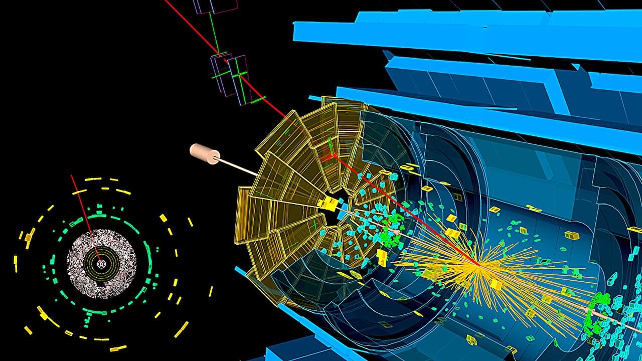
The Large Hadron Collider (LHC) is tough on electronics. Situated inside a 17-mile-long tunnel that runs in a circle under the border between Switzerland and France, this massive scientific instrument accelerates particles close to the speed of light before smashing them together. The collisions yield tiny maelstroms of particles and energy that hint at answers to fundamental questions about the building blocks of matter.
Those collisions produce an enormous amount of data—and enough radiation to scramble the bits and logic inside almost any piece of electronic equipment.
That presents a challenge to CERN’s physicists as they attempt to probe deeper into the mysteries of the Higgs boson and other fundamental particles. Off-the-shelf components simply can’t survive the harsh conditions inside the accelerator, and the market for radiation-resistant circuits is too small to entice investment from commercial chip manufacturers.
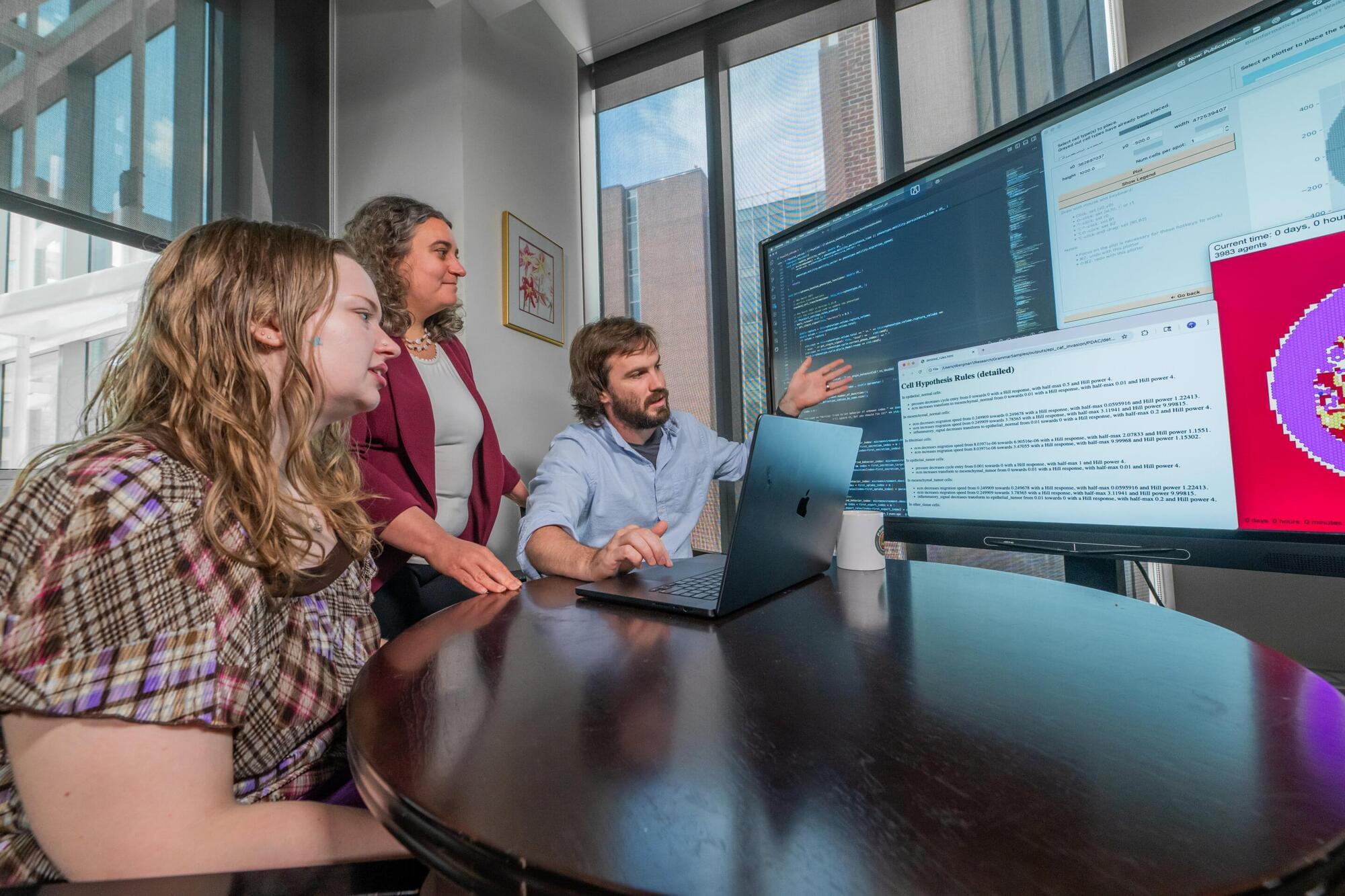
In the same vein as weather forecast models that predict developing storms, researchers have now developed a method to predict the cell activity in tissues over time. The new software combines genomics technologies with computational modeling to predict cell changes in behavior, such as communication between cells that could cause cancer cells to flourish.


Using mathematical analysis of patterns of human and animal cell behavior, scientists say they have developed a computer program that mimics the behavior of such cells in any part of the body. Led by investigators at Indiana University, Johns Hopkins Medicine, the University of Maryland School of Medicine and Oregon Health & Science University, the new work was designed to advance ways of testing and predicting biological processes, drug responses and other cell dynamics before undertaking more costly experiments with live cells.
With further work on the program, the researchers say it could eventually serve as a “digital twin” for testing any drug’s effect on cancer or other conditions, gene environment interactions during brain development, or any number of dynamic cellular molecular processes in people where such studies are not possible.
The new study and examples of cell simulations are described online July 25 in the journal Cell.

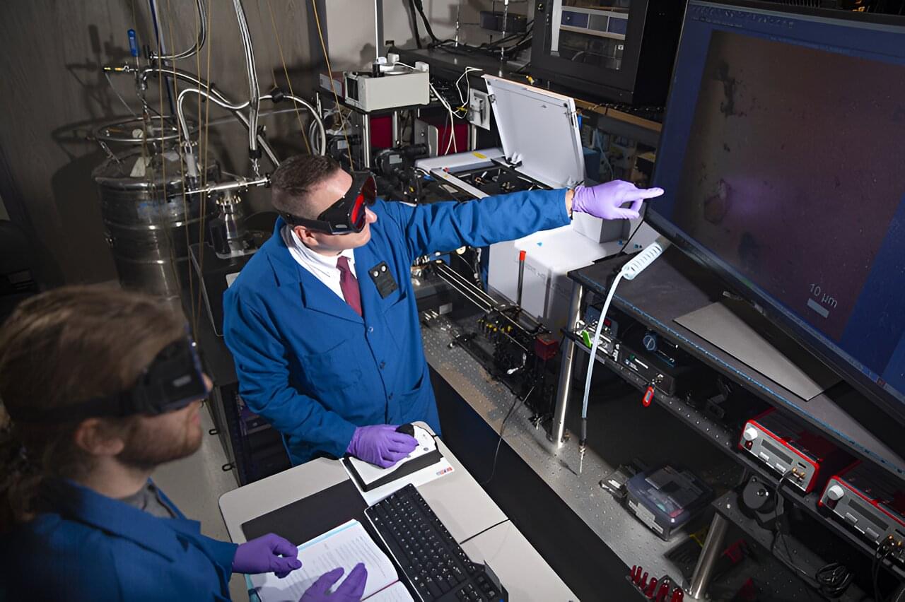
Researchers at the University of California, Irvine have discovered a new state of quantum matter. The state exists within a material that the team reports could lead to a new era of self-charging computers and ones capable of withstanding the challenges of deep space travel.
“It’s a new phase of matter, similar to how water can exist as liquid, ice or vapor,” said Luis A. Jauregui, professor of physics & astronomy at UC Irvine and corresponding author of the new paper in Physical Review Letters.
“It’s only been theoretically predicted—no one has ever measured it until now.”
New research into topological phases of matter may spur advances in innovative quantum devices. As described in a new paper published in the journal Nature Communications, a research team including Los Alamos National Laboratory scientists used a novel strain engineering approach to convert the material hafnium pentatelluride (HfTe5) to a strong topological insulator phase, increasing its bulk electrical resistance while lowering it at the surface, a key to unlocking its quantum potential.
“I’m excited that our team was able to show that the elusive and much-sought-after topological surface states can be made to become a predominant electrical conduction pathway,” said Michael Pettes, scientist with the Center for Integrated Nanotechnologies (CINT) at the Laboratory.
“This is promising for the development of types of quantum optoelectronic devices, dark matter detectors and topologically protected devices such as quantum computers. And the methodology we demonstrate is compatible for experimentation on other quantum materials.”