Toggle light / dark theme

Molecular imaging uncovers hidden flaws in plastics used for electronics

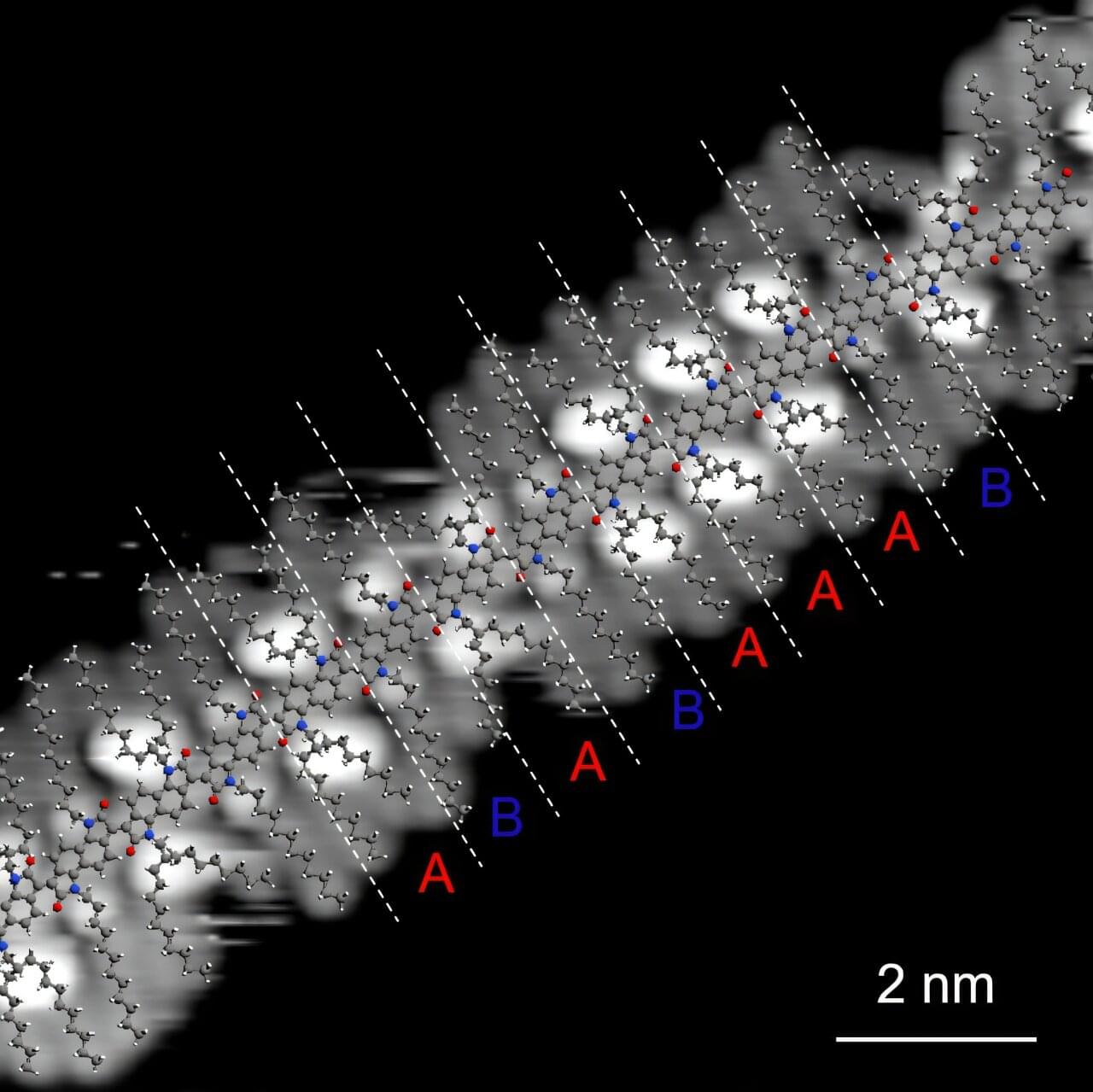
A new study uncovers revealing insights into how plastic materials used in electronics are formed, and how hidden flaws in their structure could be limiting their performance.

Conjugated polymers are a type of plastic that conduct electricity and are used in optoelectronics, computing, biosensors, and power generation. The materials are lightweight, low-cost, and can be printed in thin layers onto flexible substrates, making them ideal for next-generation technologies.

An international team of scientists investigated a popular method for making the polymers called aldol condensation, which is praised for being versatile, metal-free, environmentally friendly, and scalable.

Earth’s Gravity Might Be Warping Quantum Mechanics, Say Physicists

Scientists propose a groundbreaking experiment using quantum computers and atomic clocks to test whether gravity alters the fundamental rules of quantum theory. A recent study featured in the journal PRX Quantum reveals how a network of quantum computers equipped with optical clocks can be used t

Comparative Performance Analysis of Femtosecond-Laser-Written Diode-Pumped Pr: LiLuF4 Visible Waveguide Lasers

In crystalline materials, the fabrication of optical waveguides by femtosecond laser irradiation is not as easy as in glasses [7] because, in many cases, it is not possible to produce a refractive index increase, able to directly confine and guide light along a certain trajectory. On the contrary, the most typical situation is that the refractive index of the crystal is decreased by the effect of the high intensity of the laser, but even in those cases it can be used anyway to design efficient waveguides [22].

In our study, we designed and fabricated waveguides with different configurations and geometries in the search for the best performance, helping us to understand the confinement mechanisms in Pr: LLF. The following waveguide types were tested:

Quantum computing occurs naturally in the human brain, study finds

Kurian’s group believes these large tryptophan networks may have evolved to take advantage of their quantum properties. When cells breathe using oxygen—a process called aerobic respiration—they create free radicals, or reactive oxygen species (ROS). These unstable particles can emit high-energy UV photons, which damage DNA and other important molecules.

Tryptophan networks act as natural shields. They absorb this harmful light and re-emit it at lower energies, reducing damage. But thanks to superradiance, they may also perform this protective function much more quickly and efficiently than single molecules could.

The Progress and Trend of Heterogeneous Integration Silicon/III-V Semiconductor Optical Amplifiers

Silicon photonics is a revolutionary technology in the integrated photonics field which has experienced rapid development over the past several decades. High-quality III-V semiconductor components on Si platforms have shown their great potential to realize on-chip light-emitting sources for Si photonics with low-cost and high-density integration. In this review, we will focus on semiconductor optical amplifiers (SOAs), which have received considerable interest in diverse photonic applications. SOAs have demonstrated high performance in various on-chip optical applications through different integration technologies on Si substrates. Moreover, SOAs are also considered as promising candidates for future light sources in the wavelength tunable laser, which is one of the key suitable components in coherent optical devices.

Freestanding hafnium zirconium oxide membranes can enable advanced 2D transistors

To further reduce the size of electronic devices, while also improving their performance and energy efficiency, electronics engineers have been trying to identify alternative materials that outperform silicon and other conventional semiconductors. Two-dimensional (2D) semiconductors, materials that are just a few atoms thick and have a tunable electrical conductivity, are among the most promising candidates for the fabrication of smaller and better performing devices.

Past studies showed that these materials could be used to fabricate miniaturized transistors, electronic components that amplify or switch , particularly field-effect transistors (FETs). These are transistors that control the flow of electrical current using an electric field.

To reliably operate, however, FETs also need to integrate an insulating layer that separates the so-called gate electrode (i.e., the terminal regulating the flow of current) from the channel (i.e., the pathway through which electrical current flows). To enable greater control over the gate, this insulating layer, known as a , should have a high dielectric constant (κ), or in other words, it should effectively store electrical energy.

Computational musicology: Tracking the changing sound of bands

Coldplay, Radiohead or R.E.M.—which band has changed their music the most over the years? Professor Nick Collins from Durham University Department of Music has used a computer to try and find the answer to this by analyzing rhythm, harmony, and sound quality (known as timbre).

ASML Reportedly Faces No Tariffs on Equipment Shipments to the U.S., Allowing TSMC, Samsung & Others Ease in Establishing American Facilities

The Dutch chip equipment manufacturer will be exempted from the new US tariffs, allowing chipmakers like TSMC and Samsung easy access to lithography machines in America.

Well, the US and EU recently concluded on a trade deal, setting the tariff rates to the “baseline” 15% figure, along with potential ‘hundreds of billions’ in investments by the EU into America’s energy sector. However, there are tariff exemptions with specific categories, and one of them includes semiconductors, according to a statement released by the European Commission. This means that US companies could import chip equipment and essentials into the nation without paying the extra costs to the government in form of tariffs, and this means great news for the likes of Samsung and TSMC.

Taming Heat in Quantum Tech

Many quantum technologies function only at ultralow temperatures. Managing the flow of heat in these systems is crucial for protecting their sensitive components. Now Matteo Pioldi and his colleagues at the CNR Institute of Nanoscience and the Scuola Normale Superiore, both in Pisa, Italy, have devised a thermal analogue of a transistor that could facilitate this heat management [1]. Just as a transistor can control electric currents, the new device has the potential to control heat currents in cryogenic quantum systems.

The most common type of transistor has three electrical terminals: the source, the gate, and the drain. Adjusting the voltage applied to the gate alters the strength of the electric current flowing from the source to the drain. In the proposed device, a semiconductor-based thermal reservoir serves as the source, and metallic thermal reservoirs serve as the gate and the drain. A second semiconductor-based reservoir exchanges heat with the source through photons and with the gate and the drain through electrons. Changing the gate’s temperature affects how easily heat flows through the device and, in turn, alters the strength of the heat current flowing from the source to the drain.

Pioldi and his colleagues performed numerical simulations of their device in a realistic setup at ultralow temperatures. They found that a small change in the strength of the heat current coming from the gate could cause the strength of the current between the source and the drain to increase by an amount that was 15 times larger. They say that their device could improve heat management in quantum circuits and thus help optimize quantum sensors, quantum computers, and other temperature-sensitive quantum systems.

/* */