This is leading to even better brain engineering 👏 🙌 👌 😀 😄.
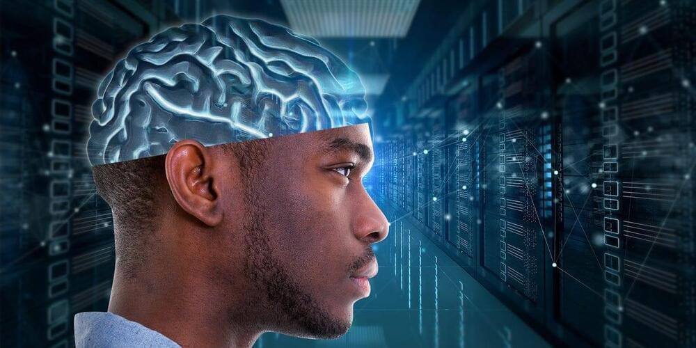
Computer-augmented brains, cures to blindness, and rebuilding the brain after injury all sound like science fiction. Today, these disruptive technologies aren’t just for Netflix, “Terminator,” and comic book fodder — in recent years, these advances are closer to reality than some might realize, and they have the ability to revolutionize neurological care.
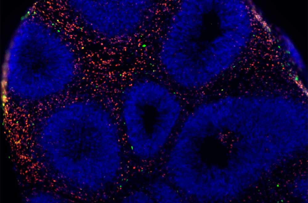
Neurologic disease is now the world’s leading cause of disability, and upwards of 11 million people have some form of permanent neurological problem from traumatic brain injuries and stroke. For example, if a traumatic brain injury has damaged the motor cortex — the region of the brain involved in voluntary movements — patients could become paralyzed, without hope of regaining full function. Or some stroke patients can suffer from aphasia, the inability to speak or understand language, due to damage to the brain regions that control speech and language comprehension.
Thanks to recent advances, sometimes lasting neurologic disease can be prevented. For example, if a stroke patient is seen quickly enough, life-threatening or-altering damage can be avoided, but it’s not always possible. Current treatments to most neurologic disease are fairly limited, as most therapies, including medications, aim to improve symptoms but can’t completely recover lost brain function.
