Scientists have spent over 25 years trying — and failing — to build computer simulations of the smallest brain we know. Today, we finally have the tools to pull it off.

Degradation of proteostasis, mitochondrial function, and cellular stress resistance results in a build-up of damaged proteins, oxidative insult, and chronic inflammation, characteristic of aging. CHIP is essential for maintaining protein quality control and cellular homeostasis by having dual E3 ubiquitin ligase and co-chaperone activities. CHIP facilitates proteostasis by maintaining proteostasis in misfolded, aggregated proteins by promoting their degradation. Mitochondrial dysfunction, oxidative imbalance, and cellular senescence are caused by its age-associated decline and contribute to neurodegenerative, cardiovascular, and oncogenic disease pathogenesis. Examples of recent pharmacological and gene-based strategies to correct CHIP and restore stress resilience have been made.
As many in the field would agree, the growing interest in two-dimensional (2D) materials is not just a trend, it reflects real progress and curiosity. Materials like graphene and MoS2 have shown fascinating behaviour, particularly because they are atomically thin and yet still possess strong electrical, optical, and mechanical properties. These features make them promising candidates for new directions in electronics. That said, turning this promise into reliable technology is still a work in progress.
This Collection focuses on how 2D materials are being developed and used in integrated electronics. The emphasis is not only on device performance, but also on the actual process of bringing these materials into practical systems. From what I have seen, some of the most exciting results come from experiments where 2D materials are added into traditional semiconductor setups, whether that is in transistors, photodetectors, or memory elements. But challenges like scalability, environmental stability, and material quality remain real obstacles.
We’re interested in contributions across the board: device demonstrations, growth techniques, interface studies, or even theoretical modelling that can guide experimental designs. For instance, studies on how these materials interact with metal contacts, or how to reduce contact resistance, are very relevant here. So are efforts to pattern or align 2D layers over large areas, which is a challenge still not fully solved.
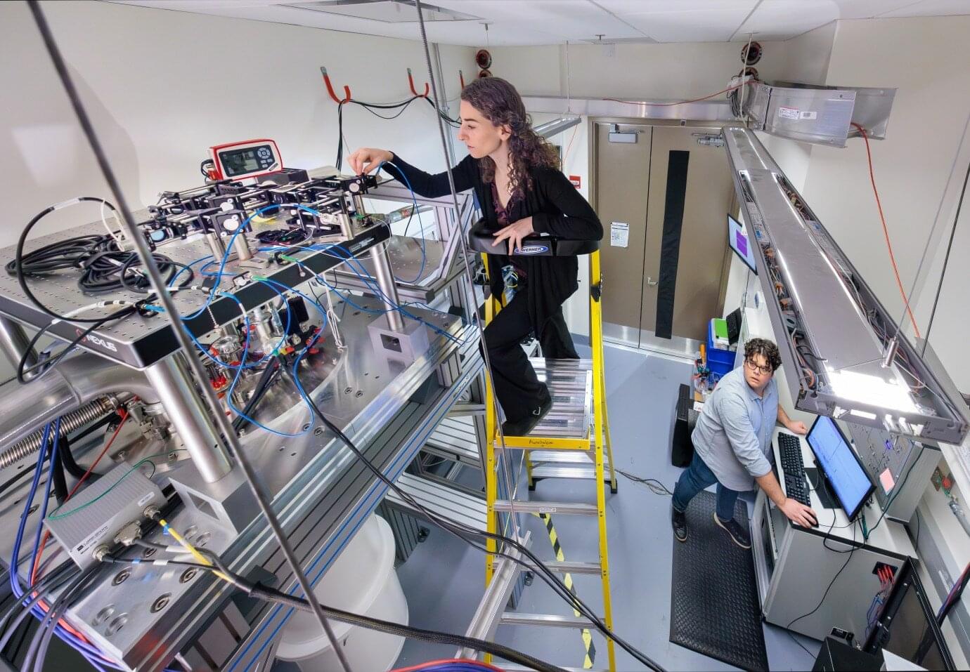
In 2024, a quantum state of light was successfully teleported through more than 30 kilometers (around 18 miles) of fiber optic cable amid a torrent of internet traffic – a feat of engineering once considered impossible.
The impressive demonstration by researchers in the US may not help you beam to work to beat the morning traffic, or download your favourite cat videos faster.
However, the ability to teleport quantum states through existing infrastructure represents a monumental step towards achieving a quantum-connected computing network, enhanced encryption, or powerful new methods of sensing.
Lasers that are fabricated directly onto silicon photonic chips offer several advantages over external laser sources, such as greater scalability. Furthermore, photonic chips with these “monolithically” integrated lasers can be commercially viable if they can be manufactured in standard semiconductor foundries.
III-V semiconductor lasers can be monolithically integrated with photonic chips by directly growing a crystalline layer of laser material, such as indium arsenide, on silicon substrate. However, photonic chips with such integrated laser source are challenging to manufacture due to mismatch between structures or properties of III-V semiconductor material and silicon. “Coupling loss” or the loss of optical power during transfer from laser source to silicon waveguides in the photonic chip is yet another concern when manufacturing photonic chips with monolithically integrated lasers.
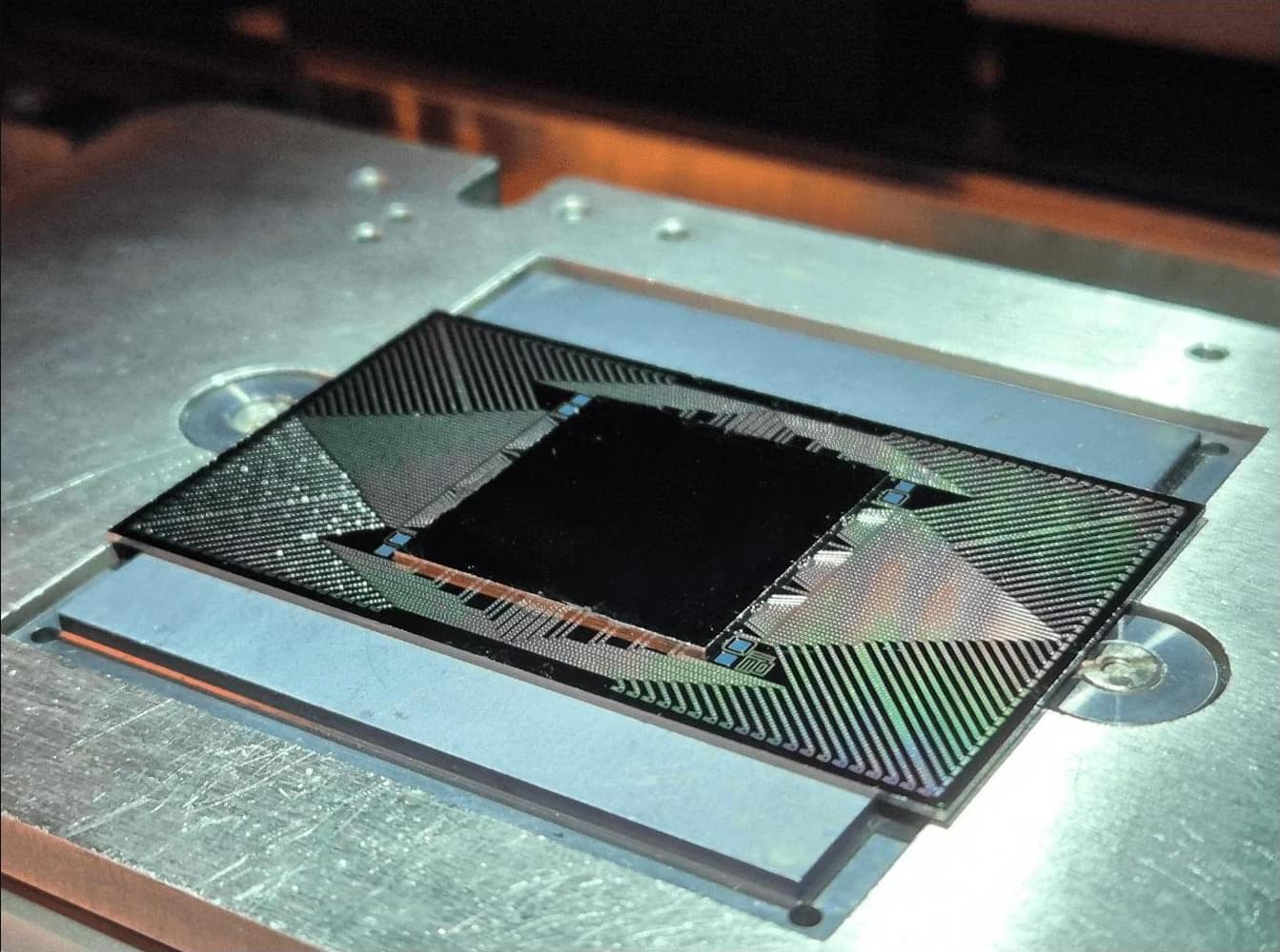
In a study that was recently published in the Journal of Lightwave Technology, Dr. Rosalyn Koscica from the University of California, United States, and her team successfully integrated indium arsenide quantum dot (QD) lasers monolithically on silicon photonics chiplets.
Research from the University of Minnesota Twin Cities gives new insight into a material that could make computer memory faster and more energy-efficient.
The study was recently published in Advanced Materials, a peer-reviewed scientific journal. The researchers also have a patent on the technology.
As technology continues to grow, so does the demand for emerging memory technology. Researchers are looking for alternatives and complements to existing memory solutions that can perform at high levels with low energy consumption to increase the functionality of everyday technology.
In the race to develop faster and more flexible wireless communication technologies, researchers are turning to an unexpected source: the same organic light-emitting diodes (OLEDs) found in smartphone screens and TVs.
A recent study by scientists at the University of St Andrews and the University of Cambridge, published in Advanced Photonics, shows that OLEDs can be engineered to transmit data at record-breaking speeds over surprisingly long distances—potentially transforming how we connect devices in the future.
The paper is titled “High-speed organic light-emitting diodes based on dinaphthylperylene achieving 4-Gbps communication.”
The intensive pursuit for quantum advantage in terms of computational complexity has further led to a modernized crucial question of when and how will quantum computers outperform classical computers. The next milestone is undoubtedly the realization of quantum acceleration in practical problems. Here we provide a clear evidence and arguments that the primary target is likely to be condensed matter physics. Our primary contributions are summarized as follows: 1) Proposal of systematic error/runtime analysis on state-of-the-art classical algorithm based on tensor networks; 2) Dedicated and high-resolution analysis on quantum resource performed at the level of executable logical instructions; 3) Clarification of quantum-classical crosspoint for ground-state simulation to be within runtime of hours using only a few hundreds of thousand physical qubits for 2d Heisenberg and 2d Fermi-Hubbard models, assuming that logical qubits are encoded via the surface code with the physical error rate of p = 10–3. To our knowledge, we argue that condensed matter problems offer the earliest platform for demonstration of practical quantum advantage that is order-of-magnitude more feasible than ever known candidates, in terms of both qubit counts and total runtime.
Yoshioka, N., Okubo, T., Suzuki, Y. et al. Hunting for quantum-classical crossover in condensed matter problems. npj Quantum Inf 10, 45 (2024). https://doi.org/10.1038/s41534-024-00839-4